- 您现在的位置:买卖IC网 > PDF目录224505 > MT46V32M16BN-5BLIT 32M X 16 DDR DRAM, 0.7 ns, PBGA60 PDF资料下载
参数资料
| 型号: | MT46V32M16BN-5BLIT |
| 元件分类: | DRAM |
| 英文描述: | 32M X 16 DDR DRAM, 0.7 ns, PBGA60 |
| 封装: | 10 X 12.50 MM, LEAD FREE, PLASTIC, FBGA-60 |
| 文件页数: | 69/82页 |
| 文件大小: | 2855K |
| 代理商: | MT46V32M16BN-5BLIT |
第1页第2页第3页第4页第5页第6页第7页第8页第9页第10页第11页第12页第13页第14页第15页第16页第17页第18页第19页第20页第21页第22页第23页第24页第25页第26页第27页第28页第29页第30页第31页第32页第33页第34页第35页第36页第37页第38页第39页第40页第41页第42页第43页第44页第45页第46页第47页第48页第49页第50页第51页第52页第53页第54页第55页第56页第57页第58页第59页第60页第61页第62页第63页第64页第65页第66页第67页第68页当前第69页第70页第71页第72页第73页第74页第75页第76页第77页第78页第79页第80页第81页第82页
512Mb: x4, x8, x16
DDR SDRAM
09005aef80a1d9e7
Micron Technology, Inc., reserves the right to change products or specifications without notice.
512MBDDRx4x8x16_2.fm - Rev. H 7/04 EN
71
2000 Micron Technology, Inc. All rights reserved.
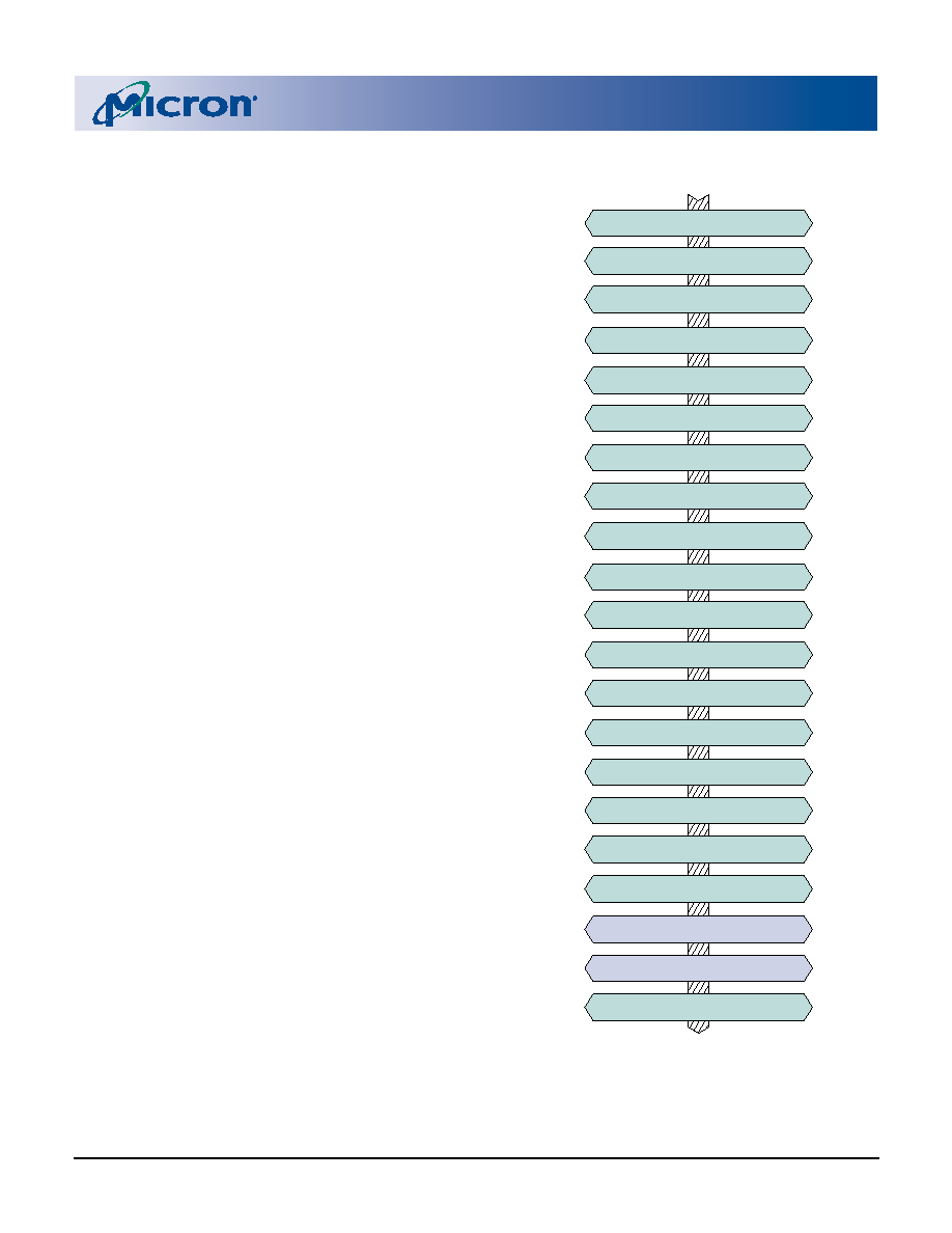
Initialization
To ensure device operation the DRAM must be ini-
tialized as described below:
1. Simultaneously apply power to VDD and VDDQ.
2. Apply VREF and then VTT power.
3. Assert and hold CKE at a LVCMOS logic low.
4. Provide stable CLOCK signals.
5. Wait at least 200s.
6. Bring CKE high and provide at least one NOP or
DESELECT command. At this point the CKE input
changes from a LVCMOS input to a SSTL2 input
only and will remain a SSTL_2 input unless a
power cycle occurs.
7. Perform a PRECHARGE ALL command.
8. Wait at least tRP time, during this time NOPs or
DESELECT commands must be given.
9. Using the LMR command program the Extended
Mode Register (E0 = 0 to enable the DLL and E1 =
0 for normal drive or E1 = 1 for reduced drive, E2
through En must be set to 0; where n = most sig-
nificant bit).
10. Wait at least tMRD time, only NOPs or DESELECT
commands are allowed.
11. Using the LMR command program the Mode Reg-
ister to set operating parameters and to reset the
DLL. Note at least 200 clock cycles are required
between a DLL reset and any READ command.
12. Wait at least tMRD time, only NOPs or DESELECT
commands are allowed.
13. Issue a PRECHARGE ALL command.
14. Wait at least tRP time, only NOPs or DESELECT
commands are allowed.
15. Issue an AUTO REFRESH command (Note this
may be moved prior to step 13).
16. Wait at least tRFC time, only NOPs or DESELECT
commands are allowed.
17. Issue an AUTO REFRESH command (Note this
may be moved prior to step 13).
18. Wait at least tRFC time, only NOPs or DESELECT
commands are allowed.
19. Although not required by the Micron device,
JEDEC requires a LMR command to clear the DLL
bit (set M8 = 0). If a LMR command is issued the
same operating parameters should be utilized as
in step 11.
20. Wait at least tMRD time, only NOPs or DESELECT
commands are allowed.
21. At this point the DRAM is ready for any valid com-
mand. Note 200 clock cycles are required between
step 11 (DLL RESET) and any READ command.
Figure 44: Initialization Flow Diagram
VDD and VDDQ Ramp
Apply VREF and VTT
CKE must be LVCMOS Low
Apply stable CLOCKs
Bring CKE High with a NOP command
Wait at least 200us
PRECHARGE ALL
Assert NOP or DESELECT for tRP time
Configure Extended Mode Register
Configure Load Mode Register and reset DLL
Assert NOP or DESELECT for tMRD time
PRECHARGE ALL
Issue AUTO REFRESH command
Assert NOP or DESELECT for tRFC time
Optional LMR command to clear DLL bit
Assert NOP or DESELECT for tMRD time
DRAM is ready for any valid command
Step
1
2
3
4
5
6
7
8
9
10
11
12
13
14
15
16
17
18
19
20
21
Assert NOP or DESELECT commands for tRFC
Issue AUTO REFRESH command
Assert NOP or DESELECT for tRP time
相关PDF资料 |
PDF描述 |
|---|---|
| MT46V32M81AZ4-6T:G | 32M X 4 DDR DRAM, 0.75 ns, PDSO66 |
| MT47H128M8HV-187ELIT:E | 128M X 8 DDR DRAM, 0.35 ns, PBGA60 |
| MT47H128M8HQ-187ELAT:E | 128M X 8 DDR DRAM, 0.35 ns, PBGA60 |
| MT48LC2M32B1TG-7 | 2M X 32 SYNCHRONOUS DRAM, 5.5 ns, PDSO86 |
| MT48LC32M4A2P-7ELIT:G | 32M X 4 SYNCHRONOUS DRAM, 5.4 ns, PDSO54 |
相关代理商/技术参数 |
参数描述 |
|---|
发布紧急采购,3分钟左右您将得到回复。