- 您现在的位置:买卖IC网 > PDF目录224505 > MT46V32M16BN-5BLIT 32M X 16 DDR DRAM, 0.7 ns, PBGA60 PDF资料下载
参数资料
| 型号: | MT46V32M16BN-5BLIT |
| 元件分类: | DRAM |
| 英文描述: | 32M X 16 DDR DRAM, 0.7 ns, PBGA60 |
| 封装: | 10 X 12.50 MM, LEAD FREE, PLASTIC, FBGA-60 |
| 文件页数: | 12/82页 |
| 文件大小: | 2855K |
| 代理商: | MT46V32M16BN-5BLIT |
第1页第2页第3页第4页第5页第6页第7页第8页第9页第10页第11页当前第12页第13页第14页第15页第16页第17页第18页第19页第20页第21页第22页第23页第24页第25页第26页第27页第28页第29页第30页第31页第32页第33页第34页第35页第36页第37页第38页第39页第40页第41页第42页第43页第44页第45页第46页第47页第48页第49页第50页第51页第52页第53页第54页第55页第56页第57页第58页第59页第60页第61页第62页第63页第64页第65页第66页第67页第68页第69页第70页第71页第72页第73页第74页第75页第76页第77页第78页第79页第80页第81页第82页
512Mb: x4, x8, x16
DDR SDRAM
09005aef80a1d9e7
Micron Technology, Inc., reserves the right to change products or specifications without notice.
512MBDDRx4x8x16_1.fm - Rev. H 7/04 EN
2
2000 Micron Technology, Inc. All rights reserved.
Figure 2: 512Mb DDR SDRAM
Part Numbers
FBGA Part Number System
Due to space limitations, FBGA-packaged compo-
nents have an abbreviated part marking that is differ-
ent from the part number. For a quick conversion of an
FBGA code, see the FBGA Part Marking Decoder on the
Micron web site www.micron.com/decoder.
General Description
The 512Mb DDR SDRAM is a high-speed CMOS,
dynamic
random-access
memory
containing
536,870,912 bits. It is internally configured as a quad-
bank DRAM.
The 512Mb DDR SDRAM uses a double data rate
architecture to achieve high-speed operation. The
double data rate architecture is essentially a 2n-
prefetch architecture with an interface designed to
transfer two data words per clock cycle at the I/O pins.
A single read or write access for the 512Mb DDR
SDRAM effectively consists of a single 2n-bit wide,
one-clock-cycle data transfer at the internal DRAM
core and two corresponding n-bit wide, one-half-
clock-cycle data transfers at the I/O pins.
A bidirectional data strobe (DQS) is transmitted
externally, along with data, for use in data capture at
the receiver. DQS is a strobe transmitted by the DDR
SDRAM during READs and by the memory controller
during WRITEs. DQS is edge-aligned with data for
READs and center-aligned with data for WRITEs. The
x16 offering has two data strobes, one for the lower
byte and one for the upper byte.
The 512Mb DDR SDRAM operates from a differen-
tial clock (CK and CK#); the crossing of CK going HIGH
and CK# going LOW will be referred to as the positive
edge of CK. Commands (address and control signals)
are registered at every positive edge of CK. Input data
is registered on both edges of DQS, and output data is
referenced to both edges of DQS, as well as to both
edges of CK.
Read and write accesses to the DDR SDRAM are
burst oriented; accesses start at a selected location and
continue for a programmed number of locations in a
programmed sequence. Accesses begin with the regis-
tration of an ACTIVE command, which is then fol-
lowed by a READ or WRITE command. The address
bits registered coincident with the ACTIVE command
are used to select the bank and row to be accessed. The
address bits registered coincident with the READ or
WRITE command are used to select the bank and the
starting column location for the burst access.
The DDR SDRAM provides for programmable READ
or WRITE burst lengths of 2, 4, or 8 locations. An auto
precharge function may be enabled to provide a self-
timed row precharge that is initiated at the end of the
burst access.
As with standard SDR SDRAMs, the pipelined,
multibank architecture of DDR SDRAMs allows for
concurrent operation, thereby providing high effective
bandwidth by hiding row precharge and activation
time.
An auto refresh mode is provided, along with a
power-saving power-down mode. All inputs are com-
patible with the JEDEC Standard for SSTL_2. All full
drive option outputs are SSTL_2, Class II compatible.
NOTE: 1. The functionality and the timing specifica-
tions discussed in this data sheet are for the
DLL-enabled mode of operation.
2. Throughout the data sheet, the various fig-
ures and text refer to DQs as “DQ.” The DQ
term is to be interpreted as any and all DQ
collectively, unless specifically stated other-
wise. Additionally, the x16 is divided into
two bytes, the lower byte and upper byte.
For the lower byte (DQ0 through DQ7) DM
refers to LDM and DQS refers to LDQS. For
the upper byte (DQ8 through DQ15) DM
refers to UDM and DQS refers to UDQS.
3. Complete
functionality
is
described
throughout the document and any page or
diagram may have been simplified to con-
vey a topic and may not be inclusive of all
requirements.
4. Any specific requirement takes precedence
over a general statement.
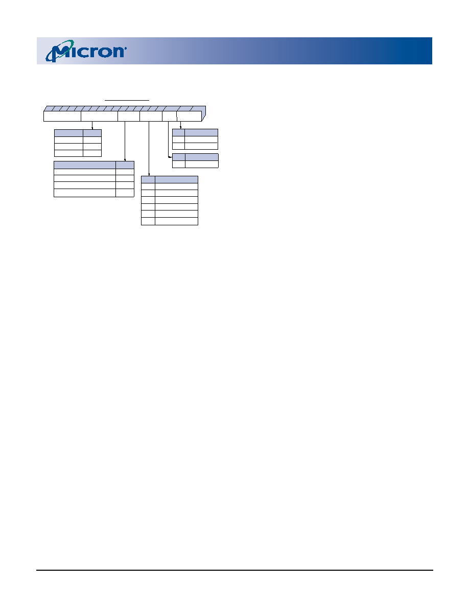
-
L
Special Options
Low Power
Configuration
MT46V
Package
Speed
Special
Options
Temperature
Configuration
128 Meg x4
64 Meg x8
32 Meg x16
128M4
64M8
32M16
Package
400 mil TSOP
400 mil TSOP Lead-Free
10 x 12.5mm FBGA
10 x 12.5mm FBGA Lead-Free
TG
P
FN
BN
Speed Grade
tCK=5ns, CL = 3
tCK=6ns, CL = 2.5
tCK=7.5ns, CL = 2
tCK=7.5ns, CL = 2.5
-5B
-6
-6T
-75E
-75Z
-75
IT
Operating Temp
Standard
Industrial Temp
Example Part Number: MT46V32M16TG-75Z
相关PDF资料 |
PDF描述 |
|---|---|
| MT46V32M81AZ4-6T:G | 32M X 4 DDR DRAM, 0.75 ns, PDSO66 |
| MT47H128M8HV-187ELIT:E | 128M X 8 DDR DRAM, 0.35 ns, PBGA60 |
| MT47H128M8HQ-187ELAT:E | 128M X 8 DDR DRAM, 0.35 ns, PBGA60 |
| MT48LC2M32B1TG-7 | 2M X 32 SYNCHRONOUS DRAM, 5.5 ns, PDSO86 |
| MT48LC32M4A2P-7ELIT:G | 32M X 4 SYNCHRONOUS DRAM, 5.4 ns, PDSO54 |
相关代理商/技术参数 |
参数描述 |
|---|
发布紧急采购,3分钟左右您将得到回复。