- 您现在的位置:买卖IC网 > PDF目录224505 > MT46V32M16BN-5BLIT 32M X 16 DDR DRAM, 0.7 ns, PBGA60 PDF资料下载
参数资料
| 型号: | MT46V32M16BN-5BLIT |
| 元件分类: | DRAM |
| 英文描述: | 32M X 16 DDR DRAM, 0.7 ns, PBGA60 |
| 封装: | 10 X 12.50 MM, LEAD FREE, PLASTIC, FBGA-60 |
| 文件页数: | 44/82页 |
| 文件大小: | 2855K |
| 代理商: | MT46V32M16BN-5BLIT |
第1页第2页第3页第4页第5页第6页第7页第8页第9页第10页第11页第12页第13页第14页第15页第16页第17页第18页第19页第20页第21页第22页第23页第24页第25页第26页第27页第28页第29页第30页第31页第32页第33页第34页第35页第36页第37页第38页第39页第40页第41页第42页第43页当前第44页第45页第46页第47页第48页第49页第50页第51页第52页第53页第54页第55页第56页第57页第58页第59页第60页第61页第62页第63页第64页第65页第66页第67页第68页第69页第70页第71页第72页第73页第74页第75页第76页第77页第78页第79页第80页第81页第82页
512Mb: x4, x8, x16
DDR SDRAM
09005aef80a1d9e7
Micron Technology, Inc., reserves the right to change products or specifications without notice.
512MBDDRx4x8x16_2.fm - Rev. H 7/04 EN
49
2000 Micron Technology, Inc. All rights reserved.
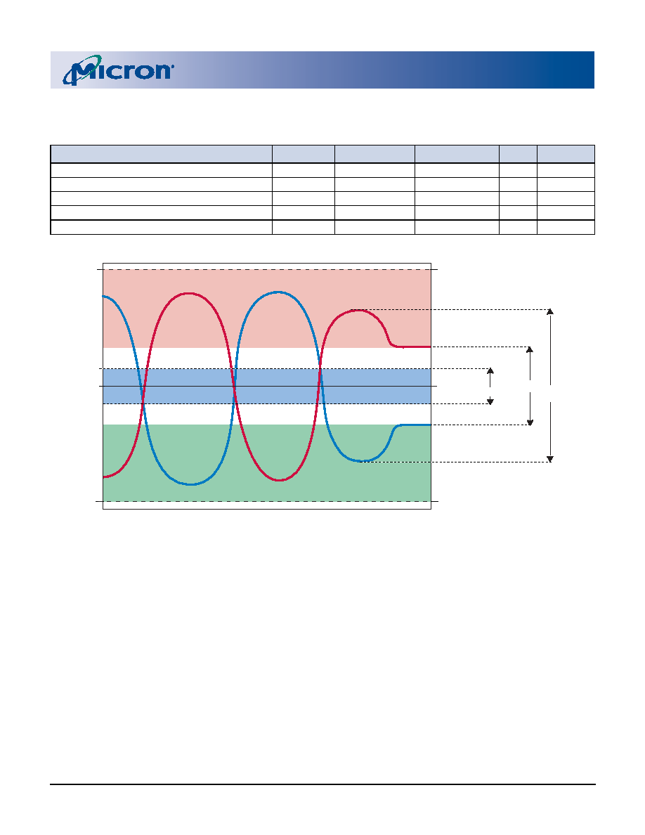
Figure 34: SSTL_2 Clock Input
NOTE:
1. This provides a minimum of 1.15V to a maximum of 1.35V, and is always half of VDDQ.
2. CK and CK# must cross in this region.
3. CK and CK# must meet at least VID(DC) min when static and is centered around VMP(DC)
4. CK and CK# must have a minimum 700mv peak to peak swing.
5. CK or CK# may not be more positive than VDDQ+ 0.3V or more negative than Vss - 0.3V.
6. For AC operation, all DC clock requirements must also be satisfied.
7. Numbers in diagram reflect nominal values non-DDR400 devices.
Table 13:
Clock Input Operating Conditions
0°C
≤ T
A ≤ +70°C; VDDQ = +2.5V ±0.2V, VDD = +2.5V ±0.2V (VDDQ = +2.6V ±0.1V, VDD = +2.6V ±0.1V for DDR400)
PARAMETER/CONDITION
SYMBOL
MIN
MAX
UNITS
NOTES
Clock Input Mid-Point Voltage; CK and CK#
VMP(DC)
1.15
1.35
V
Clock Input Voltage Level; CK and CK#
VIN(DC)
-0.3
VDDQ + 0.3
Clock Input Differential Voltage; CK and CK#
VID(DC)
0.36
VDDQ + 0.6
Clock Input Differential Voltage; CK and CK#
VID(AC)
0.7
VDDQ + 0.6
Clock Input Crossing Point Voltage; CK and CK#
VIX(AC)
0.5 x VDDQ - 0.2 0.5 x VDDQ + 0.2
CK
CK#
2.80V
2
3
5
Maximum Clock Level
Minimum Clock Level
4
- 0.30V
1.25V
1.45V
1.05V
VID (AC)
VID (DC)
X
1
VMP (DC)
VIX (AC)
X
相关PDF资料 |
PDF描述 |
|---|---|
| MT46V32M81AZ4-6T:G | 32M X 4 DDR DRAM, 0.75 ns, PDSO66 |
| MT47H128M8HV-187ELIT:E | 128M X 8 DDR DRAM, 0.35 ns, PBGA60 |
| MT47H128M8HQ-187ELAT:E | 128M X 8 DDR DRAM, 0.35 ns, PBGA60 |
| MT48LC2M32B1TG-7 | 2M X 32 SYNCHRONOUS DRAM, 5.5 ns, PDSO86 |
| MT48LC32M4A2P-7ELIT:G | 32M X 4 SYNCHRONOUS DRAM, 5.4 ns, PDSO54 |
相关代理商/技术参数 |
参数描述 |
|---|
发布紧急采购,3分钟左右您将得到回复。