- 您现在的位置:买卖IC网 > PDF目录4046 > MT42L128M32D2MH-3 IT:A (Micron Technology Inc)IC LPDDR2 SDRAM 4GBIT 134FBGA PDF资料下载
参数资料
| 型号: | MT42L128M32D2MH-3 IT:A |
| 厂商: | Micron Technology Inc |
| 文件页数: | 116/164页 |
| 文件大小: | 0K |
| 描述: | IC LPDDR2 SDRAM 4GBIT 134FBGA |
| 标准包装: | 1,000 |
| 格式 - 存储器: | RAM |
| 存储器类型: | 移动 LPDDR2 SDRAM |
| 存储容量: | 4G(128M x 32) |
| 速度: | 333MHz |
| 接口: | 并联 |
| 电源电压: | 1.14 V ~ 1.3 V |
| 工作温度: | -25°C ~ 85°C |
| 封装/外壳: | 134-VFBGA |
| 供应商设备封装: | 134-FBGA(11x11.5) |
| 包装: | 散装 |
第1页第2页第3页第4页第5页第6页第7页第8页第9页第10页第11页第12页第13页第14页第15页第16页第17页第18页第19页第20页第21页第22页第23页第24页第25页第26页第27页第28页第29页第30页第31页第32页第33页第34页第35页第36页第37页第38页第39页第40页第41页第42页第43页第44页第45页第46页第47页第48页第49页第50页第51页第52页第53页第54页第55页第56页第57页第58页第59页第60页第61页第62页第63页第64页第65页第66页第67页第68页第69页第70页第71页第72页第73页第74页第75页第76页第77页第78页第79页第80页第81页第82页第83页第84页第85页第86页第87页第88页第89页第90页第91页第92页第93页第94页第95页第96页第97页第98页第99页第100页第101页第102页第103页第104页第105页第106页第107页第108页第109页第110页第111页第112页第113页第114页第115页当前第116页第117页第118页第119页第120页第121页第122页第123页第124页第125页第126页第127页第128页第129页第130页第131页第132页第133页第134页第135页第136页第137页第138页第139页第140页第141页第142页第143页第144页第145页第146页第147页第148页第149页第150页第151页第152页第153页第154页第155页第156页第157页第158页第159页第160页第161页第162页第163页第164页
�� �
�
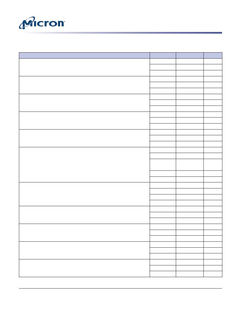
�2Gb:� x16,� x32� Mobile� LPDDR2� SDRAM� S4�
�Electrical� Specifications� –� I� DD� Specifications� and� Conditions�
�Table� 59:� I� DD� Specification� Parameters� and� Operating� Conditions� (Continued)�
�Notes� 1–3� apply� to� all� parameters� and� conditions�
�Parameter/Condition�
�Idle� power-down� standby� current� with� clock� stop:� CK� =� LOW,� CK#� =�
�HIGH;� CKE� is� LOW;� CS#� is� HIGH;� All� banks� are� idle;� CA� bus� inputs� are� stable;�
�Data� bus� inputs� are� stable�
�Idle� non-power-down� standby� current:� t� CK� =� t� CKmin;� CKE� is� HIGH;� CS#� is�
�HIGH;� All� banks� are� idle;� CA� bus� inputs� are� switching;� Data� bus� inputs� are� sta-�
�ble�
�Idle� non-power-down� standby� current� with� clock� stopped:� CK� =� LOW;�
�CK#� =� HIGH;� CKE� is� HIGH;� CS#� is� HIGH;� All� banks� are� idle;� CA� bus� inputs� are�
�stable;� Data� bus� inputs� are� stable�
�Symbol�
�I� DD2PS1�
�I� DD2PS2�
�I� DD2PS,in�
�I� DD2N1�
�I� DD2N2�
�I� DD2N,in�
�I� DD2NS1�
�I� DD2NS2�
�I� DD2NS,in�
�Power Supply�
�V� DD1�
�V� DD2�
�V� DDCA� ,� V� DDQ�
�V� DD1�
�V� DD2�
�V� DDCA� ,� V� DDQ�
�V� DD1�
�V� DD2�
�V� DDCA� ,� V� DDQ�
�Notes�
�4�
�4�
�4�
�Active� power-down� standby� current:�
�t� CK�
�=�
�t� CKmin;�
�CKE� is� LOW;� CS#� is�
�I� DD3P1�
�V� DD1�
�HIGH;� One� bank� is� active;� CA� bus� inputs� are� switching;� Data� bus� inputs� are�
�stable�
�Active� power-down� standby� current� with� clock� stop:� CK� =� LOW,� CK#� =�
�HIGH;� CKE� is� LOW;� CS#� is� HIGH;� One� bank� is� active;� CA� bus� inputs� are� stable;�
�Data� bus� inputs� are� stable�
�Active� non-power-down� standby� current:� t� CK� =� t� CKmin;� CKE� is� HIGH;� CS#�
�is� HIGH;� One� bank� is� active;� CA� bus� inputs� are� switching;� Data� bus� inputs� are�
�stable�
�Active� non-power-down� standby� current� with� clock� stopped:� CK� =�
�LOW,� CK#� =� HIGH� CKE� is� HIGH;� CS#� is� HIGH;� One� bank� is� active;� CA� bus� inputs�
�are� stable;� Data� bus� inputs� are� stable�
�I� DD3P2�
�I� DD3P,in�
�I� DD3PS1�
�I� DD3PS2�
�I� DD3PS,in�
�I� DD3N1�
�I� DD3N2�
�I� DD3N,in�
�I� DD3NS1�
�I� DD3NS2�
�I� DD3NS,in�
�V� DD2�
�V� DDCA� ,� V� DDQ�
�V� DD1�
�V� DD2�
�V� DDCA� ,� V� DDQ�
�V� DD1�
�V� DD2�
�V� DDCA� ,� V� DDQ�
�V� DD1�
�V� DD2�
�V� DDCA� ,� V� DDQ�
�4�
�4�
�4�
�4�
�Operating� burst� READ� current:�
�t� CK�
�=�
�t� CKmin;�
�CS#� is� HIGH� between� valid�
�I� DD4R1�
�V� DD1�
�commands;� One� bank� is� active;� BL� =� 4;� RL� =� RL� (MIN);� CA� bus� inputs� are�
�switching;� 50%� data� change� each� burst� transfer�
�I� DD4R2�
�I� DD4R,in�
�V� DD2�
�V� DDCA�
�I� DD4RQ�
�V� DDQ�
�5�
�Operating� burst� WRITE� current:�
�t� CK�
�=�
�t� CKmin;�
�CS#� is� HIGH� between� valid�
�I� DD4W1�
�V� DD1�
�commands;� One� bank� is� active;� BL� =� 4;� WL� =� WLmin;� CA� bus� inputs� are� switch-�
�ing;� 50%� data� change� each� burst� transfer�
�I� DD4W2�
�I� DD4W,in�
�V� DD2�
�V� DDCA� ,� V� DDQ�
�4�
�All-bank� REFRESH� burst� current:�
�t� CK�
�=�
�t� CKmin;�
�CKE� is� HIGH� between� valid�
�I� DD51�
�V� DD1�
�commands;� t� RC� =� t� RFCabmin;� Burst� refresh;� CA� bus� inputs� are� switching;� Data�
�bus� inputs� are� stable�
�All-bank� REFRESH� average� current:� t� CK� =� t� CKmin;� CKE� is� HIGH� between�
�valid� commands;� t� RC� =� t� REFI;� CA� bus� inputs� are� switching;� Data� bus� inputs� are�
�stable�
�I� DD52�
�I� DD5IN�
�I� DD5AB1�
�I� DD5AB2�
�I� DD5AB,in�
�V� DD2�
�V� DDCA� ,� V� DDQ�
�V� DD1�
�V� DD2�
�V� DDCA� ,� V� DDQ�
�4�
�4�
�Per-bank� REFRESH� average� current:�
�t� CK�
�=�
�t� CKmin;�
�CKE� is� HIGH� between�
�I� DD5PB1�
�V� DD1�
�6�
�valid� commands;� t� RC� =� t� REFI/8;� CA� bus� inputs� are� switching;� Data� bus� inputs�
�are� stable�
�I� DD5PB2�
�I� DD5PB,in�
�V� DD2�
�V� DDCA� ,� V� DDQ�
�6�
�4,� 6�
�PDF:� 09005aef83f3f2eb�
�2gb_mobile_lpddr2_s4_g69a.pdf� –� Rev.� N� 3/12� EN�
�116�
�Micron� Technology,� Inc.� reserves� the� right� to� change� products� or� specifications� without� notice.�
�2010� Micron� Technology,� Inc.� All� rights� reserved.�
�相关PDF资料 |
PDF描述 |
|---|---|
| FMM43DRKF | CONN EDGECARD 86POS DIP .156 SLD |
| FMC44DRXS-S734 | CONN EDGECARD 88POS DIP .100 SLD |
| ABB105DHAN | CONN EDGECARD 210PS R/A .050 SLD |
| ABB105DHAD | CONN EDGECARD 210PS R/A .050 SLD |
| MT42L128M32D2KL-3 IT:A | IC LPDDR2 SDRAM 4GBIT 168FBGA |
相关代理商/技术参数 |
参数描述 |
|---|
发布紧急采购,3分钟左右您将得到回复。