- 您现在的位置:买卖IC网 > PDF目录385639 > MT46V8M8 (Micron Technology, Inc.) 2 Meg x 8 x 4 banks DDR SDRAM(2 M x 8 x 4组,双数据速率同步动态RAM) PDF资料下载
参数资料
| 型号: | MT46V8M8 |
| 厂商: | Micron Technology, Inc. |
| 英文描述: | 2 Meg x 8 x 4 banks DDR SDRAM(2 M x 8 x 4组,双数据速率同步动态RAM) |
| 中文描述: | 2梅格× 8 × 4银行DDR SDRAM内存(2米× 8 × 4组,双数据速率同步动态RAM)的 |
| 文件页数: | 16/69页 |
| 文件大小: | 2369K |
| 代理商: | MT46V8M8 |
第1页第2页第3页第4页第5页第6页第7页第8页第9页第10页第11页第12页第13页第14页第15页当前第16页第17页第18页第19页第20页第21页第22页第23页第24页第25页第26页第27页第28页第29页第30页第31页第32页第33页第34页第35页第36页第37页第38页第39页第40页第41页第42页第43页第44页第45页第46页第47页第48页第49页第50页第51页第52页第53页第54页第55页第56页第57页第58页第59页第60页第61页第62页第63页第64页第65页第66页第67页第68页第69页
16
64Mb: x4, x8, x16 DDR SDRAM
64Mx4x8x16DDR_B.p65
–
Rev. B; Pub. 10/00
Micron Technology, Inc., reserves the right to change products or specifications without notice.
2000, Micron Technology, Inc.
64Mb: x4, x8, x16
DDR SDRAM
Operations
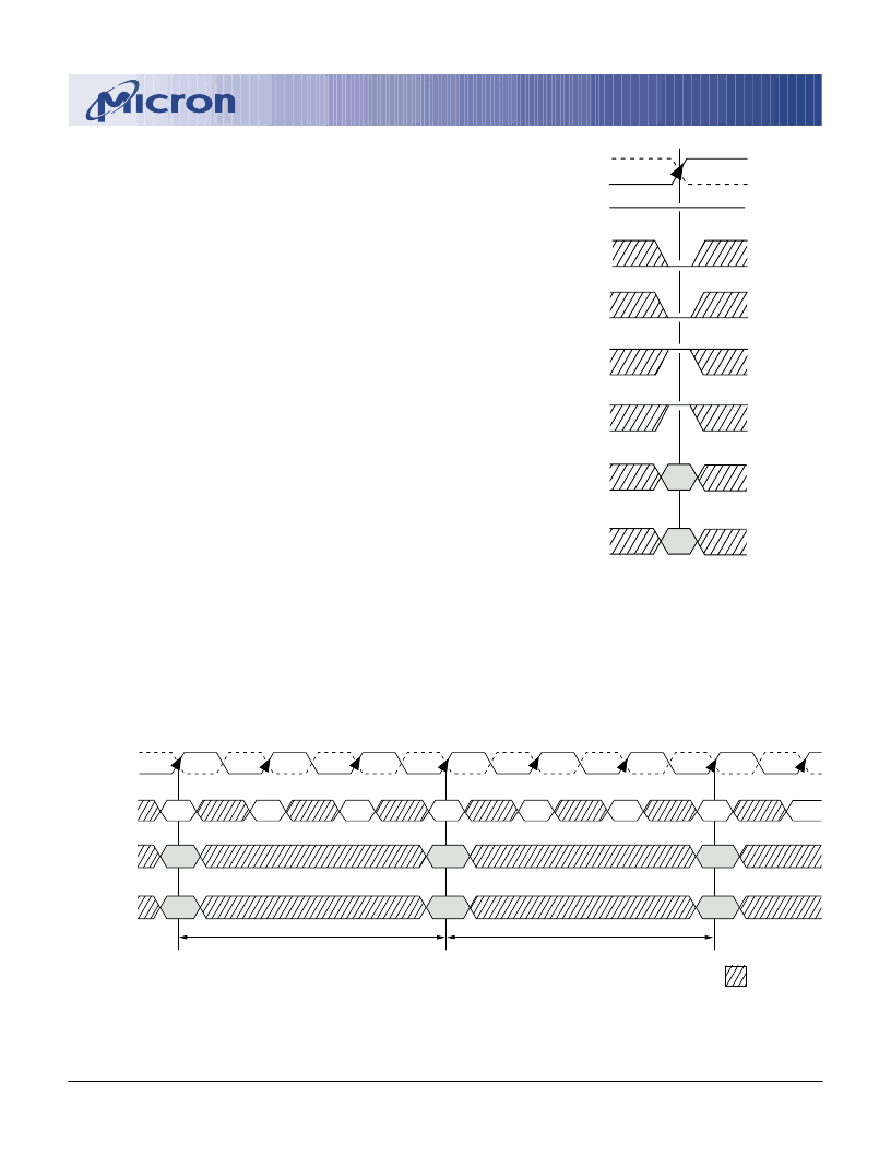
BANK/ROW ACTIVATION
Before any READ or WRITE commands can be
issued to a bank within the DDR SDRAM, a row in that
bank must be “opened.” This is accomplished via the
ACTIVE command, which selects both the bank and
the row to be activated, as shown in Figure 4.
After a row is opened with an ACTIVE command,
a READ or WRITE command may be issued to that
row, subject to the
t
RCD specification.
t
RCD (MIN)
should be divided by the clock period and rounded up
to the next whole number to determine the earliest
clock edge after the ACTIVE command on which a
READ or WRITE command can be entered. For ex-
ample, a
t
RCD specification of 20ns with a 133 MHz
clock (7.5ns period) results in 2.7 clocks rounded to 3.
This is reflected in Figure 5, which covers any case where
2 <
t
RCD (MIN)/
t
CK
≤
3. (Figure 5 also shows the same
case for
t
RCD; the same procedure is used to convert
other specification limits from time units to clock
cycles).
A subsequent ACTIVE command to a different row
in the same bank can only be issued after the previous
active row has been “closed” (precharged). The mini-
mum time interval between successive ACTIVE com-
mands to the same bank is defined by
t
RC.
A subsequent ACTIVE command to another bank
can be issued while the first bank is being accessed,
which results in a reduction of total row-access over-
head. The minimum time interval between successive
ACTIVE commands to different banks is defined by
t
RRD.
Figure 5
Example: Meeting
t
RCD (
t
RRD) MIN When 2 <
t
RCD (
t
RRD) MIN/
t
CK
≤
3
Figure 4
Activating a Specific Row in
a Specific Bank
CS#
WE#
CAS#
RAS#
CKE
A0-A11
RA
RA = Row Address
BA = Bank Address
HIGH
BA0,1
BA
CK
CK#
COMMAND
BA0, BA1
ACT
ACT
NOP
tRRD
tRCD
CK
CK#
Bank
x
Bank
y
A0-A11
Row
Row
NOP
RD/WR
NOP
Bank
y
Col
NOP
T0
T1
T2
T3
T4
T5
T6
T7
DON
’
T CARE
NOP
相关PDF资料 |
PDF描述 |
|---|---|
| MT46V2M32LG | DOUBLE DATA RATE DDR SDRAM |
| MT46V2M32V1 | DOUBLE DATA RATE DDR SDRAM |
| MT46V32M4-1 | DOUBLE DATA RATE DDR SDRAM |
| MT46V32M4TG-75 | DOUBLE DATA RATE DDR SDRAM |
| MT46V32M4TG-75L | DOUBLE DATA RATE DDR SDRAM |
相关代理商/技术参数 |
参数描述 |
|---|---|
| MT46VDCFG-T16A | 制造商:Micron Technology Inc 功能描述:SDRAM DDR SPECIAL/CUSTOM 46VDC FBGA 2.5V PLASTIC 256MEG - Trays |
| MT470 | 制造商:MARKTECH 制造商全称:Marktech Corporate 功能描述:TRUNCATED LED LAMPS |
| MT4700CF-UBL | 制造商:MARKTECH 制造商全称:Marktech Corporate 功能描述:Blue Visible Emitter |
| MT470-G | 制造商:MARKTECH 制造商全称:Marktech Corporate 功能描述:TRUNCATED LED LAMPS |
| MT470-R | 制造商:MARKTECH 制造商全称:Marktech Corporate 功能描述:TRUNCATED LED LAMPS |
发布紧急采购,3分钟左右您将得到回复。