- 您现在的位置:买卖IC网 > PDF目录98046 > MTD20N06HDT4 (MOTOROLA INC) 20 A, 60 V, 0.045 ohm, N-CHANNEL, Si, POWER, MOSFET PDF资料下载
参数资料
| 型号: | MTD20N06HDT4 |
| 厂商: | MOTOROLA INC |
| 元件分类: | JFETs |
| 英文描述: | 20 A, 60 V, 0.045 ohm, N-CHANNEL, Si, POWER, MOSFET |
| 文件页数: | 1/12页 |
| 文件大小: | 274K |
| 代理商: | MTD20N06HDT4 |
1
Motorola TMOS Power MOSFET Transistor Device Data
Designer's Data Sheet
HDTMOS E-FET.
Power Field Effect Transistor
DPAK for Surface Mount
N–Channel Enhancement–Mode Silicon Gate
This advanced HDTMOS power FET is designed to withstand
high energy in the avalanche and commutation modes. This new
energy efficient design also offers a drain–to–source diode with a
fast recovery time. Designed for low voltage, high speed switching
applications in power supplies, converters and PWM motor
controls, these devices are particularly well suited for bridge circuits
where diode speed and commutating safe operating areas are
critical and offer additional safety margin against unexpected
voltage transients.
Avalanche Energy Specified
Source–to–Drain Diode Recovery Time Comparable to a Discrete
Fast Recovery Diode
Diode is Characterized for Use in Bridge Circuits
IDSS and VDS(on) Specified at Elevated Temperature
Surface Mount Package Available in 16 mm, 13–inch/2500
Unit Tape & Reel, Add T4 Suffix to Part Number
MAXIMUM RATINGS (TC = 25°C unless otherwise noted)
Rating
Symbol
Value
Unit
Drain–Source Voltage
VDSS
60
Vdc
Drain–Gate Voltage (RGS = 1.0 M)
VDGR
60
Vdc
Gate–Source Voltage — Continuous
Gate–Source Voltage — Non–Repetitive (tp ≤ 10 ms)
VGS
VGSM
± 20
± 30
Vdc
Vpk
Drain Current — Continuous
Drain Current — Continuous @ 100
°C
Drain Current — Single Pulse (tp ≤ 10 s)
ID
IDM
20
16
60
Adc
Apk
Total Power Dissipation
Derate above 25
°C
Total Power Dissipation @ TA = 25°C, when mounted to minimum recommended pad size
PD
40
0.32
1.75
Watts
W/
°C
Watts
Operating and Storage Temperature Range
TJ, Tstg
– 55 to 150
°C
Single Pulse Drain–to–Source Avalanche Energy — Starting TJ = 25°C
(VDD = 25 Vdc, VGS = 10 Vdc, Peak IL = 20 Apk, L = 0.3 mH, RG = 25 )
EAS
60
mJ
Thermal Resistance — Junction to Case
Thermal Resistance — Junction to Ambient
Thermal Resistance — Junction to Ambient, when mounted with the minimum recommended pad size
R
θJC
R
θJA
R
θJA
3.13
100
71.4
°C/W
Maximum Lead Temperature for Soldering Purposes, 1/8
″ from case for 10 seconds
TL
260
°C
Designer’s Data for “Worst Case” Conditions — The Designer’s Data Sheet permits the design of most circuits entirely from the information presented. SOA Limit
curves — representing boundaries on device characteristics — are given to facilitate “worst case” design.
E–FET, Designer’s and HDTMOS are trademarks of Motorola, Inc. TMOS is a registered trademark of Motorola, Inc.
Thermal Clad is a trademark of the Bergquist Company.
Preferred devices are Motorola recommended choices for future use and best overall value.
REV 2
Order this document
by MTD20N06HD/D
MOTOROLA
SEMICONDUCTOR TECHNICAL DATA
Motorola, Inc. 1995
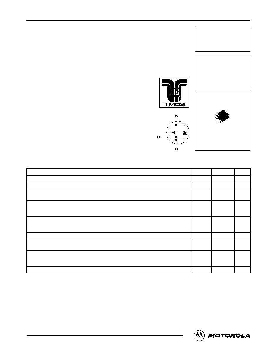
MTD20N06HD
TMOS POWER FET
20 AMPERES
60 VOLTS
RDS(on) = 0.045 OHM
Motorola Preferred Device
D
S
G
CASE 369A–13, Style 2
DPAK
相关PDF资料 |
PDF描述 |
|---|---|
| MTD20P03HDLT4 | 19 A, 30 V, 0.099 ohm, P-CHANNEL, Si, POWER, MOSFET |
| MTD20P06HDLT4 | 20 A, 60 V, 0.15 ohm, P-CHANNEL, Si, POWER, MOSFET |
| MTD2955ET4 | 12 A, 60 V, 0.3 ohm, P-CHANNEL, Si, POWER, MOSFET |
| MTD2955VT4 | 12 A, 60 V, 0.23 ohm, P-CHANNEL, Si, POWER, MOSFET |
| MTD2N40E | 2 A, 400 V, 3.5 ohm, N-CHANNEL, Si, POWER, MOSFET |
相关代理商/技术参数 |
参数描述 |
|---|---|
| MTD20N06V | 制造商:MOTOROLA 制造商全称:Motorola, Inc 功能描述:TMOS POWER FET 20 AMPERES 60 VOLTS RDS(on) = 0.080 OHM |
| MTD20N06VT4 | 功能描述:MOSFET 60V 20A N-Channel RoHS:否 制造商:STMicroelectronics 晶体管极性:N-Channel 汲极/源极击穿电压:650 V 闸/源击穿电压:25 V 漏极连续电流:130 A 电阻汲极/源极 RDS(导通):0.014 Ohms 配置:Single 最大工作温度: 安装风格:Through Hole 封装 / 箱体:Max247 封装:Tube |
| MTD20P03 | 制造商:MOTOROLA 制造商全称:Motorola, Inc 功能描述:TMOS POWER FET LOGIC LEVEL 19 AMPERES 30 VOLTS RDS(on) = 0.099 OHM |
| MTD20P03HDL | 制造商:MOTOROLA 制造商全称:Motorola, Inc 功能描述:TMOS POWER FET LOGIC LEVEL 19 AMPERES 30 VOLTS RDS(on) = 0.099 OHM |
| MTD20P03HDL1 | 制造商:ON Semiconductor 功能描述:Trans MOSFET P-CH 30V 19A 3-Pin(3+Tab) IPAK Rail 制造商:Rochester Electronics LLC 功能描述:- Bulk |
发布紧急采购,3分钟左右您将得到回复。