- 您现在的位置:买卖IC网 > PDF目录98046 > MTD20N06HDT4 (MOTOROLA INC) 20 A, 60 V, 0.045 ohm, N-CHANNEL, Si, POWER, MOSFET PDF资料下载
参数资料
| 型号: | MTD20N06HDT4 |
| 厂商: | MOTOROLA INC |
| 元件分类: | JFETs |
| 英文描述: | 20 A, 60 V, 0.045 ohm, N-CHANNEL, Si, POWER, MOSFET |
| 文件页数: | 9/12页 |
| 文件大小: | 274K |
| 代理商: | MTD20N06HDT4 |
MTD20N06HD
6
Motorola TMOS Power MOSFET Transistor Device Data
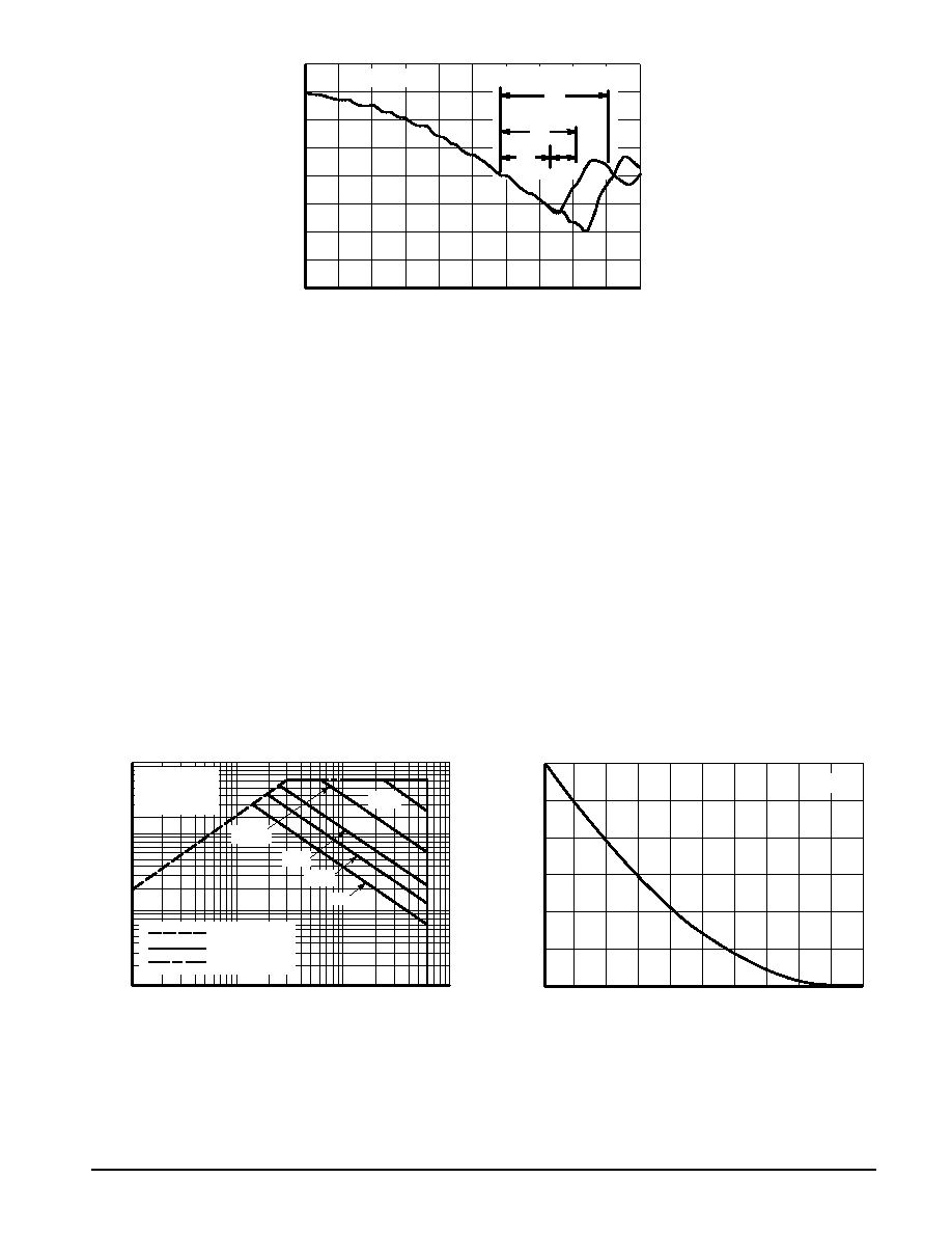
I S
,SOURCE
CURRENT
t, TIME
Figure 10. Reverse Recovery Time (trr)
di/dt = 300 A/
s
Standard Cell Density
High Cell Density
tb
trr
ta
trr
SAFE OPERATING AREA
The Forward Biased Safe Operating Area curves define
the maximum simultaneous drain–to–source voltage and
drain current that a transistor can handle safely when it is
forward biased. Curves are based upon maximum peak junc-
tion temperature and a case temperature (TC) of 25°C. Peak
repetitive pulsed power limits are determined by using the
thermal response data in conjunction with the procedures
discussed in AN569, “Transient Thermal Resistance – Gen-
eral Data and Its Use.”
Switching between the off–state and the on–state may tra-
verse any load line provided neither rated peak current (IDM)
nor rated voltage (VDSS) is exceeded, and that the transition
time (tr, tf) does not exceed 10 s. In addition the total power
averaged over a complete switching cycle must not exceed
(TJ(MAX) – TC)/(R
θJC).
A power MOSFET designated E–FET can be safely used
in switching circuits with unclamped inductive loads. For reli-
able operation, the stored energy from circuit inductance dis-
sipated in the transistor while in avalanche must be less than
the rated limit and must be adjusted for operating conditions
differing from those specified. Although industry practice is to
rate in terms of energy, avalanche energy capability is not a
constant. The energy rating decreases non–linearly with an
increase of peak current in avalanche and peak junction tem-
perature.
Although many E–FETs can withstand the stress of drain–
to–source avalanche at currents up to rated pulsed current
(IDM), the energy rating is specified at rated continuous cur-
rent (ID), in accordance with industry custom. The energy
rating must be derated for temperature as shown in the ac-
companying graph (Figure 12). Maximum energy at currents
below rated continuous ID can safely be assumed to equal
the values indicated.
VDS, DRAIN–TO–SOURCE VOLTAGE (VOLTS)
I D
,DRAIN
CURRENT
(AMPS)
E
AS
,SINGLE
PULSE
DRAIN–T
O–SOURCE
A
V
ALANCHE
ENERGY
(mJ)
TJ, STARTING JUNCTION TEMPERATURE (°C)
Figure 11. Maximum Rated Forward Biased
Safe Operating Area
0
25
50
75
100
125
40
60
20
10
30
150
50
0.1
1.0
100
1.0
0.1
10
Figure 12. Maximum Avalanche Energy versus
Starting Junction Temperature
10
s
100
s
1 ms
dc
10 ms
ID = 20 A
VGS = 20 V
SINGLE PULSE
TC = 25°C
RDS(on) LIMIT
THERMAL LIMIT
PACKAGE LIMIT
相关PDF资料 |
PDF描述 |
|---|---|
| MTD20P03HDLT4 | 19 A, 30 V, 0.099 ohm, P-CHANNEL, Si, POWER, MOSFET |
| MTD20P06HDLT4 | 20 A, 60 V, 0.15 ohm, P-CHANNEL, Si, POWER, MOSFET |
| MTD2955ET4 | 12 A, 60 V, 0.3 ohm, P-CHANNEL, Si, POWER, MOSFET |
| MTD2955VT4 | 12 A, 60 V, 0.23 ohm, P-CHANNEL, Si, POWER, MOSFET |
| MTD2N40E | 2 A, 400 V, 3.5 ohm, N-CHANNEL, Si, POWER, MOSFET |
相关代理商/技术参数 |
参数描述 |
|---|---|
| MTD20N06V | 制造商:MOTOROLA 制造商全称:Motorola, Inc 功能描述:TMOS POWER FET 20 AMPERES 60 VOLTS RDS(on) = 0.080 OHM |
| MTD20N06VT4 | 功能描述:MOSFET 60V 20A N-Channel RoHS:否 制造商:STMicroelectronics 晶体管极性:N-Channel 汲极/源极击穿电压:650 V 闸/源击穿电压:25 V 漏极连续电流:130 A 电阻汲极/源极 RDS(导通):0.014 Ohms 配置:Single 最大工作温度: 安装风格:Through Hole 封装 / 箱体:Max247 封装:Tube |
| MTD20P03 | 制造商:MOTOROLA 制造商全称:Motorola, Inc 功能描述:TMOS POWER FET LOGIC LEVEL 19 AMPERES 30 VOLTS RDS(on) = 0.099 OHM |
| MTD20P03HDL | 制造商:MOTOROLA 制造商全称:Motorola, Inc 功能描述:TMOS POWER FET LOGIC LEVEL 19 AMPERES 30 VOLTS RDS(on) = 0.099 OHM |
| MTD20P03HDL1 | 制造商:ON Semiconductor 功能描述:Trans MOSFET P-CH 30V 19A 3-Pin(3+Tab) IPAK Rail 制造商:Rochester Electronics LLC 功能描述:- Bulk |
发布紧急采购,3分钟左右您将得到回复。