- 您现在的位置:买卖IC网 > PDF目录98046 > MTD20N06HDT4 (MOTOROLA INC) 20 A, 60 V, 0.045 ohm, N-CHANNEL, Si, POWER, MOSFET PDF资料下载
参数资料
| 型号: | MTD20N06HDT4 |
| 厂商: | MOTOROLA INC |
| 元件分类: | JFETs |
| 英文描述: | 20 A, 60 V, 0.045 ohm, N-CHANNEL, Si, POWER, MOSFET |
| 文件页数: | 11/12页 |
| 文件大小: | 274K |
| 代理商: | MTD20N06HDT4 |
MTD20N06HD
8
Motorola TMOS Power MOSFET Transistor Device Data
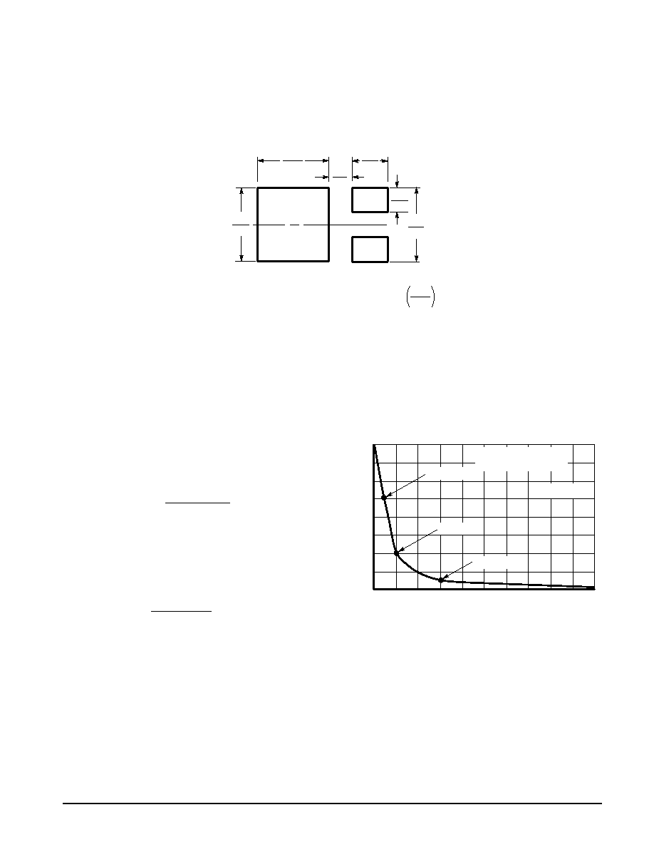
INFORMATION FOR USING THE DPAK SURFACE MOUNT PACKAGE
RECOMMENDED FOOTPRINT FOR SURFACE MOUNTED APPLICATIONS
Surface mount board layout is a critical portion of the total
design. The footprint for the semiconductor packages must be
the correct size to ensure proper solder connection interface
between the board and the package. With the correct pad
geometry, the packages will self align when subjected to a
solder reflow process.
0.190
4.826
mm
inches
0.100
2.54
0.063
1.6
0.165
4.191
0.118
3.0
0.243
6.172
POWER DISSIPATION FOR A SURFACE MOUNT DEVICE
The power dissipation for a surface mount device is a
function of the drain pad size.
These can vary from the
minimum pad size for soldering to a pad size given for
maximum power dissipation. Power dissipation for a surface
mount device is determined by TJ(max), the maximum rated
junction temperature of the die, R
θJA, the thermal resistance
from the device junction to ambient, and the operating
temperature, TA. Using the values provided on the data sheet,
PD can be calculated as follows:
PD =
TJ(max) – TA
R
θJA
The values for the equation are found in the maximum
ratings table on the data sheet. Substituting these values into
the equation for an ambient temperature TA of 25°C, one can
calculate the power dissipation of the device. For a DPAK
device, PD is calculated as follows.
PD =
150
°C – 25°C
71.4
°C/W
= 1.75 Watts
The 71.4
°C/W for the DPAK package assumes the use of
the recommended footprint on a glass epoxy printed circuit
board to achieve a power dissipation of 1.75 Watts. There are
other alternatives to achieving higher power dissipation from
the surface mount packages. One is to increase the area of the
drain pad. By increasing the area of the drain pad, the power
dissipation can be increased. Although one can almost double
the power dissipation with this method, one will be giving up
area on the printed circuit board which can defeat the purpose
of using surface mount technology. For example, a graph of
R
θJA versus drain pad area is shown in Figure 15.
Figure 15. Thermal Resistance versus Drain Pad
Area for the DPAK Package (Typical)
1.75 Watts
Board Material = 0.0625
″
G–10/FR–4, 2 oz Copper
80
100
60
40
20
10
8
6
4
2
0
3.0 Watts
5.0 Watts
TA = 25°C
A, AREA (SQUARE INCHES)
T
O
AMBIENT
(
C/W)°
R
JA
,THERMAL
RESIST
ANCE,
JUNCTION
θ
Another alternative would be to use a ceramic substrate or
an aluminum core board such as Thermal Clad
. Using a
board material such as Thermal Clad, an aluminum core
board, the power dissipation can be doubled using the same
footprint.
相关PDF资料 |
PDF描述 |
|---|---|
| MTD20P03HDLT4 | 19 A, 30 V, 0.099 ohm, P-CHANNEL, Si, POWER, MOSFET |
| MTD20P06HDLT4 | 20 A, 60 V, 0.15 ohm, P-CHANNEL, Si, POWER, MOSFET |
| MTD2955ET4 | 12 A, 60 V, 0.3 ohm, P-CHANNEL, Si, POWER, MOSFET |
| MTD2955VT4 | 12 A, 60 V, 0.23 ohm, P-CHANNEL, Si, POWER, MOSFET |
| MTD2N40E | 2 A, 400 V, 3.5 ohm, N-CHANNEL, Si, POWER, MOSFET |
相关代理商/技术参数 |
参数描述 |
|---|---|
| MTD20N06V | 制造商:MOTOROLA 制造商全称:Motorola, Inc 功能描述:TMOS POWER FET 20 AMPERES 60 VOLTS RDS(on) = 0.080 OHM |
| MTD20N06VT4 | 功能描述:MOSFET 60V 20A N-Channel RoHS:否 制造商:STMicroelectronics 晶体管极性:N-Channel 汲极/源极击穿电压:650 V 闸/源击穿电压:25 V 漏极连续电流:130 A 电阻汲极/源极 RDS(导通):0.014 Ohms 配置:Single 最大工作温度: 安装风格:Through Hole 封装 / 箱体:Max247 封装:Tube |
| MTD20P03 | 制造商:MOTOROLA 制造商全称:Motorola, Inc 功能描述:TMOS POWER FET LOGIC LEVEL 19 AMPERES 30 VOLTS RDS(on) = 0.099 OHM |
| MTD20P03HDL | 制造商:MOTOROLA 制造商全称:Motorola, Inc 功能描述:TMOS POWER FET LOGIC LEVEL 19 AMPERES 30 VOLTS RDS(on) = 0.099 OHM |
| MTD20P03HDL1 | 制造商:ON Semiconductor 功能描述:Trans MOSFET P-CH 30V 19A 3-Pin(3+Tab) IPAK Rail 制造商:Rochester Electronics LLC 功能描述:- Bulk |
发布紧急采购,3分钟左右您将得到回复。