- 您现在的位置:买卖IC网 > PDF目录19108 > MTP50P03HDLG (ON Semiconductor)MOSFET P-CH 30V 50A TO220AB PDF资料下载
参数资料
| 型号: | MTP50P03HDLG |
| 厂商: | ON Semiconductor |
| 文件页数: | 6/8页 |
| 文件大小: | 0K |
| 描述: | MOSFET P-CH 30V 50A TO220AB |
| 产品目录绘图: | MOSFET TO-220, TO-220AB |
| 标准包装: | 50 |
| FET 型: | MOSFET P 通道,金属氧化物 |
| FET 特点: | 逻辑电平门 |
| 漏极至源极电压(Vdss): | 30V |
| 电流 - 连续漏极(Id) @ 25° C: | 50A |
| 开态Rds(最大)@ Id, Vgs @ 25° C: | 25 毫欧 @ 25A,5V |
| Id 时的 Vgs(th)(最大): | 2V @ 250µA |
| 闸电荷(Qg) @ Vgs: | 100nC @ 5V |
| 输入电容 (Ciss) @ Vds: | 4900pF @ 25V |
| 功率 - 最大: | 125W |
| 安装类型: | 通孔 |
| 封装/外壳: | TO-220-3 |
| 供应商设备封装: | TO-220AB |
| 包装: | 管件 |
| 产品目录页面: | 1558 (CN2011-ZH PDF) |
| 其它名称: | MTP50P03HDLGOS |
�� �
�
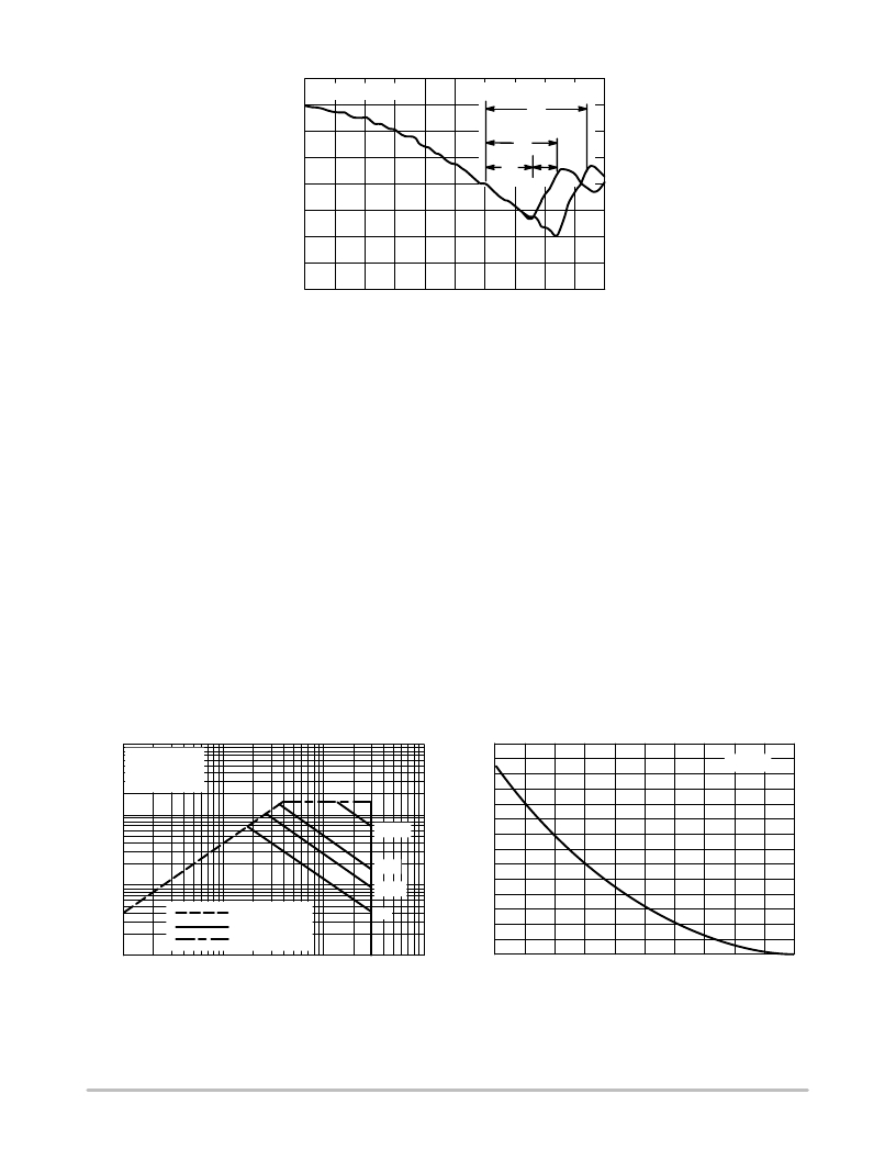
�MTP50P03HDL�
�di/dt = 300 A/� m� s�
�Standard� Cell� Density�
�t� rr�
�High� Cell� Density�
�t� a�
�t� rr�
�t� b�
�t,� TIME�
�Figure� 11.� Reverse� Recovery� Time� (t� rr� )�
�SAFE� OPERATING� AREA�
�The� Forward� Biased� Safe� Operating� Area� curves� define�
�the� maximum� simultaneous� drain?to?source� voltage� and�
�drain� current� that� a� transistor� can� handle� safely� when� it� is�
�forward� biased.� Curves� are� based� upon� maximum� peak�
�junction� temperature� and� a� case� temperature� (T� C� )� of� 25� °� C.�
�Peak� repetitive� pulsed� power� limits� are� determined� by� using�
�the� thermal� response� data� in� conjunction� with� the� procedures�
�discussed� in� AN569,� “Transient� Thermal� Resistance� ?�
�General� Data� and� Its� Use.”�
�Switching� between� the� off?state� and� the� on?state� may�
�traverse� any� load� line� provided� neither� rated� peak� current�
�(I� DM� )� nor� rated� voltage� (V� DSS� )� is� exceeded,� and� that� the�
�transition� time� (t� r� ,� t� f� )� does� not� exceed� 10� m� s.� In� addition� the�
�total� power� averaged� over� a� complete� switching� cycle� must�
�not� exceed� (T� J(MAX)� ?� T� C� )/(R� q� JC� ).�
�A� power� MOSFET� designated� E?FET� can� be� safely� used�
�in� switching� circuits� with� unclamped� inductive� loads.� For�
�1000�
�reliable� operation,� the� stored� energy� from� circuit� inductance�
�dissipated� in� the� transistor� while� in� avalanche� must� be� less�
�than� the� rated� limit� and� must� be� adjusted� for� operating�
�conditions� differing� from� those� specified.� Although� industry�
�practice� is� to� rate� in� terms� of� energy,� avalanche� energy�
�capability� is� not� a� constant.� The� energy� rating� decreases�
�non?linearly� with� an� increase� of� peak� current� in� avalanche�
�and� peak� junction� temperature.�
�Although� many� E?FETs� can� withstand� the� stress� of�
�drain?to?source� avalanche� at� currents� up� to� rated� pulsed�
�current� (I� DM� ),� the� energy� rating� is� specified� at� rated�
�continuous� current� (I� D� ),� in� accordance� with� industry�
�custom.� The� energy� rating� must� be� derated� for� temperature�
�as� shown� in� the� accompanying� graph� (Figure� 13).� Maximum�
�energy� at� currents� below� rated� continuous� I� D� can� safely� be�
�assumed� to� equal� the� values� indicated.�
�1400�
�100�
�V� GS� =� 20� V�
�SINGLE� PULSE�
�T� C� =� 25� °� C�
�100� m� s�
�1� ms�
�1200�
�1000�
�800�
�600�
�I� D� = 50 A�
�10�
�10 ms�
�400�
�R� DS(on)� LIMIT�
�THERMAL� LIMIT�
�PACKAGE� LIMIT�
�dc�
�200�
�1�
�0.1�
�1.0�
�10�
�100�
�0�
�25�
�50�
�75�
�100�
�125�
�150�
�V� DS� ,� DRAIN?TO?SOURCE� VOLTAGE� (VOLTS)�
�Figure� 12.� Maximum� Rated� Forward� Biased�
�Safe� Operating� Area�
�T� J� ,� STARTING� JUNCTION� TEMPERATURE� (� °� C)�
�Figure� 13.� Maximum� Avalanche� Energy� versus�
�Starting� Junction� Temperature�
�http://onsemi.com�
�6�
�相关PDF资料 |
PDF描述 |
|---|---|
| 553-0118F | LED CBI 3MM BI-LVL RED/BLUE |
| 553-0128F | LED 3MM BI LEVEL GRN/BLUE PC MNT |
| 553-0182F | LED CBI 3MM BI-LVL BLUE/GREEN |
| 5530182F | LED GRN/BLU BI-LEVEL |
| 550-2404-807F | LED CBI 5MM RED DIFF VERT SGL |
相关代理商/技术参数 |
参数描述 |
|---|---|
| MTP50P03HDLG | 制造商:ON Semiconductor 功能描述:MOSFET P TO-220 |
| MTP50S | 制造商:NELLSEMI 制造商全称:Nell Semiconductor Co., Ltd 功能描述:Three-Phase Bridge Rectifier, 50A |
| MTP50W | 制造商:NELLSEMI 制造商全称:Nell Semiconductor Co., Ltd 功能描述:Glass Passivated Triple-Phase Bridge Rectifier, 50A |
| MTP5210F3 | 制造商:CYSTEKEC 制造商全称:Cystech Electonics Corp. 功能描述:P-Channel Enhancement Mode Power MOSFET |
| MTP52K3BPNO | 功能描述:插线板 3 1/2 UNWIRED IDC B RoHS:否 制造商:Switchcraft 产品类型:Bantam (TT) 正规化: 高度/机架数量: 深度: 端接类型: 位置/触点数量:48 |
发布紧急采购,3分钟左右您将得到回复。