- 您现在的位置:买卖IC网 > Datasheet目录482 > MTW32N20EG (ON Semiconductor)MOSFET N-CH 200V 32A TO247 Datasheet资料下载
参数资料
| 型号: | MTW32N20EG |
| 厂商: | ON Semiconductor |
| 文件页数: | 2/7页 |
| 文件大小: | 0K |
| 描述: | MOSFET N-CH 200V 32A TO247 |
| 产品变化通告: | 1Q2012 Discontinuation 30/Mar/2012 |
| 产品目录绘图: | MOSFET TO-247AE |
| 标准包装: | 30 |
| FET 型: | MOSFET N 通道,金属氧化物 |
| FET 特点: | 标准 |
| 漏极至源极电压(Vdss): | 200V |
| 电流 - 连续漏极(Id) @ 25° C: | 32A |
| 开态Rds(最大)@ Id, Vgs @ 25° C: | 75 毫欧 @ 16A,10V |
| Id 时的 Vgs(th)(最大): | 4V @ 250µA |
| 闸电荷(Qg) @ Vgs: | 120nC @ 10V |
| 输入电容 (Ciss) @ Vds: | 5000pF @ 25V |
| 功率 - 最大: | 180W |
| 安装类型: | 通孔 |
| 封装/外壳: | TO-247-3 |
| 供应商设备封装: | TO-247 |
| 包装: | 管件 |
| 产品目录页面: | 1558 (CN2011-ZH PDF) |
| 其它名称: | MTW32N20EGOS |
�� �
�
�MTW32N20E�
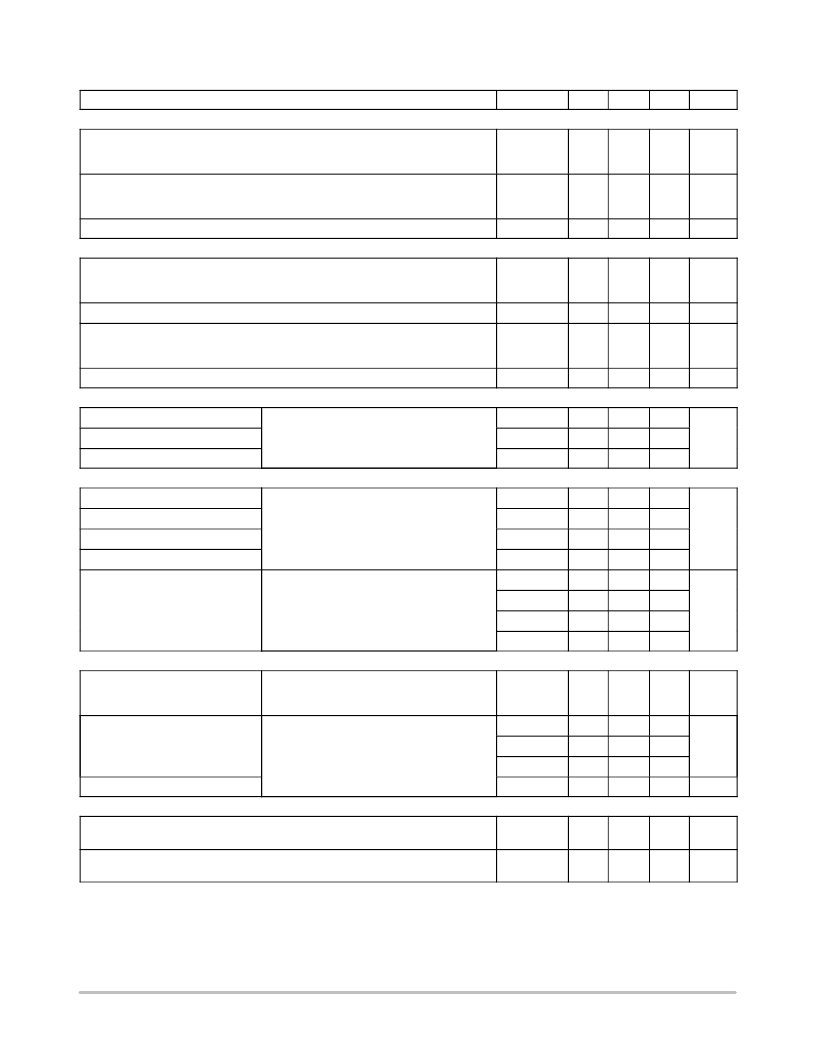
�ELECTRICAL� CHARACTERISTICS� (T� J� =� 25� °� C� unless� otherwise� noted)�
�Characteristic�
�Symbol�
�Min�
�Typ�
�Max�
�Unit�
�OFF� CHARACTERISTICS�
�Drain� ?� Source� Breakdown� Voltage�
�(V� GS� =� 0� V,� I� D� =� 250� m� Adc)�
�Temperature� Coefficient� (Positive)�
�Zero� Gate� Voltage� Drain� Current�
�(V� DS� =� 200� Vdc,� V� GS� =� 0)�
�(V� DS� =� 200� Vdc,� V� GS� =� 0,� T� J� =� 125� °� C)�
�Gate� ?� Body� Leakage� Current� (V� GS� =� ±� 20� Vdc,� V� DS� =� 0)�
�V� (BR)DSS�
�I� DSS�
�I� GSS�
�200�
�?�
�?�
�?�
�?�
�?�
�247�
�?�
�?�
�?�
�?�
�?�
�250�
�1000�
�100�
�Vdc�
�mV/� °� C�
�m� Adc�
�nAdc�
�ON� CHARACTERISTICS� (Note� 1)�
�Gate� Threshold� Voltage�
�(V� DS� =� V� GS� ,� I� D� =� 250� m� Adc)�
�Temperature� Coefficient� (Negative)�
�Static� Drain� ?� Source� On� ?� Resistance� (V� GS� =� 10� Vdc,� I� D� =� 16� Adc)�
�Drain� ?� Source� On� ?� Voltage� (V� GS� =� 10� Vdc)�
�(I� D� =� 32� Adc)�
�(I� D� =� 16� Adc,� T� J� =� 125� °� C)�
�Forward� Transconductance� (V� DS� =� 15� Vdc,� I� D� =� 16� Adc)�
�V� GS(th)�
�R� DS(on)�
�V� DS(on)�
�g� FS�
�2.0�
�?�
�?�
�?�
�?�
�12�
�?�
�8.0�
�0.064�
�?�
�?�
�?�
�4.0�
�?�
�0.075�
�3.0�
�2.7�
�?�
�Vdc�
�mV/� °� C�
�W�
�Vdc�
�mhos�
�DYNAMIC� CHARACTERISTICS�
�Input� Capacitance�
�C� iss�
�?�
�3600�
�5000�
�pF�
�Output� Capacitance�
�Reverse� Transfer� Capacitance�
�(V� DS� =� 25� Vdc,� V� GS� =� 0,� f� =� 1.0� MHz)�
�C� oss�
�C� rss�
�?�
�?�
�690�
�130�
�1000�
�250�
�SWITCHING� CHARACTERISTICS� (Notes� 1� &� 2)�
�Turn� ?� On� Delay� Time�
�t� d(on)�
�?�
�25�
�50�
�ns�
�Rise� Time�
�Turn� ?� Off� Delay� Time�
�Fall� Time�
�(V� DD� =� 100� Vdc,� I� D� =� 32� Adc,�
�V� GS� =� 10� Vdc,� R� G� =� 6.2� W� )�
�t� r�
�t� d(off)�
�t� f�
�?�
�?�
�?�
�120�
�75�
�91�
�240�
�150�
�182�
�Gate� Charge�
�(V� DS� =� 160� Vdc,� I� D� =� 32� Adc,�
�V� GS� =� 10� Vdc)�
�Q� T�
�Q� 1�
�Q� 2�
�Q� 3�
�?�
�?�
�?�
�?�
�85�
�12�
�40�
�30�
�120�
�?�
�?�
�?�
�nC�
�SOURCE� ?� DRAIN� DIODE� CHARACTERISTICS� (Note� 1)�
�Forward� On� ?� Voltage�
�Reverse� Recovery� Time�
�Reverse� Recovery� Stored� Charge�
�(I� S� =� 32� Adc,� V� GS� =� 0)�
�(I� S� =� 16� Adc,� V� GS� =� 0,� T� J� =� 125� °� C)�
�(I� S� =� 32� Adc,� V� GS� =� 0,� dI� S� /dt� =� 100� A/� m� s)�
�V� SD�
�t� rr�
�t� a�
�t� b�
�Q� RR�
�?�
�?�
�?�
�?�
�?�
�?�
�1.1�
�0.9�
�280�
�195�
�85�
�2.94�
�2.0�
�?�
�?�
�?�
�?�
�?�
�Vdc�
�ns�
�m� C�
�INTERNAL� PACKAGE� INDUCTANCE�
�Internal� Drain� Inductance�
�(Measured� from� the� drain� lead� 0.25� ″� from� package� to� center� of� die)�
�Internal� Source� Inductance�
�(Measured� from� the� source� lead� 0.25� ″� from� package� to� source� bond� pad)�
�L� D�
�L� S�
�?�
�?�
�5.0�
�13�
�?�
�?�
�nH�
�nH�
�1.� Pulse� Test:� Pulse� Width� ≤� 300� m� s,� Duty� Cycle� ≤� 2%.�
�2.� Switching� characteristics� are� independent� of� operating� junction� temperature.�
�http://onsemi.com�
�2�
�相关PDF资料 |
PDF描述 |
|---|---|
| MTY100N10E | MOSFET N-CH 100V 100A TO-264 |
| MV37509MP6 | LED SS HE RED ORN CLEAR PCB 5MM |
| MV53164 | LED BARGRAPH 10-SEG YELLOW |
| MV5377C | LED SS YELLOW DIFFUSED PCB 3MM |
| MV57173 | LED PANEL IND SS DUAL LP HE RED |
相关代理商/技术参数 |
参数描述 |
|---|---|
| MTW32N25 | 制造商:MOTOROLA 制造商全称:Motorola, Inc 功能描述:TMOS POWER FET 32 AMPERES 250 VOLTS RDS(on) = 0.08 OHM |
| MTW32N25E | 制造商:MOTOROLA 制造商全称:Motorola, Inc 功能描述:TMOS POWER FET 32 AMPERES 250 VOLTS RDS(on) = 0.08 OHM |
| MTW33N10E | 制造商:MOTOROLA 制造商全称:Motorola, Inc 功能描述:TMOS POWER FET 33 AMPERES 100 VOLTS RDS(on) = 0.06 OHM |
| MTW35N15E | 制造商:MOTOROLA 制造商全称:Motorola, Inc 功能描述:TMOS POWER FET 35 AMPERES 150 VOLTS RDS(on) = 0.05 OHM |
| MTW45N10 | 制造商:MOTOROLA 制造商全称:Motorola, Inc 功能描述:TMOS POWER FET 45 AMPERES 100 VOLTS RDS(on) = 0.035 OHM |
发布紧急采购,3分钟左右您将得到回复。