- 您现在的位置:买卖IC网 > Datasheet目录482 > MTW32N20EG (ON Semiconductor)MOSFET N-CH 200V 32A TO247 Datasheet资料下载
参数资料
| 型号: | MTW32N20EG |
| 厂商: | ON Semiconductor |
| 文件页数: | 5/7页 |
| 文件大小: | 0K |
| 描述: | MOSFET N-CH 200V 32A TO247 |
| 产品变化通告: | 1Q2012 Discontinuation 30/Mar/2012 |
| 产品目录绘图: | MOSFET TO-247AE |
| 标准包装: | 30 |
| FET 型: | MOSFET N 通道,金属氧化物 |
| FET 特点: | 标准 |
| 漏极至源极电压(Vdss): | 200V |
| 电流 - 连续漏极(Id) @ 25° C: | 32A |
| 开态Rds(最大)@ Id, Vgs @ 25° C: | 75 毫欧 @ 16A,10V |
| Id 时的 Vgs(th)(最大): | 4V @ 250µA |
| 闸电荷(Qg) @ Vgs: | 120nC @ 10V |
| 输入电容 (Ciss) @ Vds: | 5000pF @ 25V |
| 功率 - 最大: | 180W |
| 安装类型: | 通孔 |
| 封装/外壳: | TO-247-3 |
| 供应商设备封装: | TO-247 |
| 包装: | 管件 |
| 产品目录页面: | 1558 (CN2011-ZH PDF) |
| 其它名称: | MTW32N20EGOS |
�� �
�
�MTW32N20E�
�20�
�16�
�V� DS�
�T� J� =� 25� °� C�
�I� D� =� 32� A�
�V� DS� =� 160� V�
�200�
�180�
�160�
�140�
�1000�
�200�
�100�
�T� J� =� 25� °� C�
�I� D� =� 32� A�
�V� DD� =� 100� V�
�V� GS� =� 10� V�
�t� d(off)�
�t� d(on)�
�t� r�
�t� f�
�12�
�Q� T�
�120�
�100�
�8�
�Q� 1�
�Q� 2�
�V� GS�
�80�
�60�
�20�
�10�
�4�
�40�
�0�
�0�
�10�
�Q� 3�
�20�
�30� 40� 50� 60� 70�
�80�
�90�
�20�
�0�
�100�
�2�
�1�
�1�
�2�
�10�
�20�
�100�
�Q� T� ,� TOTAL� CHARGE� (nC)�
�Figure� 8.� Gate� ?� To� ?� Source� and� Drain� ?� To� ?� Source�
�Voltage� versus� Total� Charge�
�R� G� ,� GATE� RESISTANCE� (OHMS)�
�Figure� 9.� Resistive� Switching� Time�
�Variation� versus� Gate� Resistance�
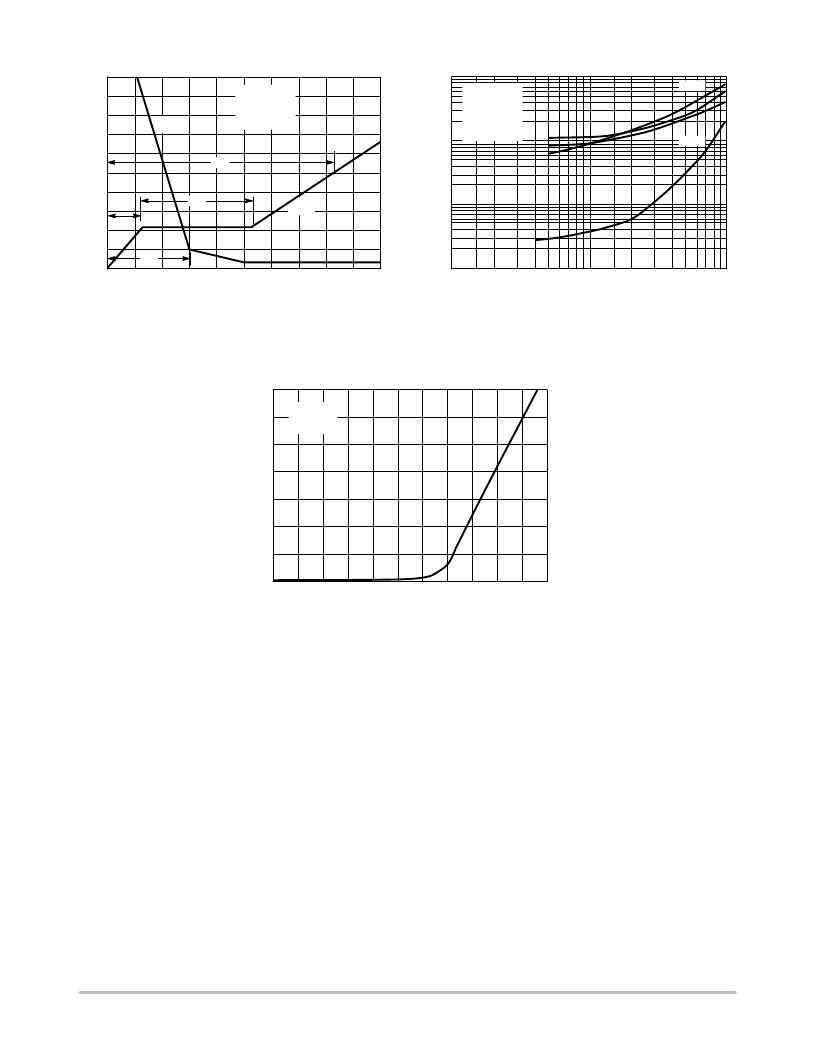
�DRAIN� ?� TO� ?� SOURCE� DIODE� CHARACTERISTICS�
�30�
�20�
�10�
�T� J� =� 25� °� C�
�V� GS� =� 0� V�
�0�
�0�
�0.2� 0.4� 0.6� 0.8� 1�
�V� SD� ,� SOURCE-TO-DRAIN� VOLTAGE� (VOLTS)�
�Figure� 10.� Diode� Forward� Voltage� versus� Current�
�SAFE� OPERATING� AREA�
�The� Forward� Biased� Safe� Operating� Area� curves� define� the�
�maximum� simultaneous� drain� ?� to� ?� source� voltage� and� drain�
�current� that� a� transistor� can� handle� safely� when� it� is� forward�
�biased.� Curves� are� based� upon� maximum� peak� junction�
�temperature� and� a� case� temperature� (T� C� )� of� 25� °� C.� Peak�
�repetitive� pulsed� power� limits� are� determined� by� using� the�
�thermal� response� data� in� conjunction� with� the� procedures�
�discussed� in� AN569,� “Transient� Thermal� Resistance� ?� General�
�Data� and� Its� Use.”�
�Switching� between� the� off� ?� state� and� the� on� ?� state� may�
�traverse� any� load� line� provided� neither� rated� peak� current�
�(I� DM� )� nor� rated� voltage� (V� DSS� )� is� exceeded� and� the�
�transition� time� (t� r� ,t� f� )� do� not� exceed� 10� m� s.� In� addition� the� total�
�power� averaged� over� a� complete� switching� cycle� must� not�
�exceed� (T� J(MAX)� ?� T� C� )/(R� q� JC� ).�
�A� Power� MOSFET� designated� E� ?� FET� can� be� safely� used�
�reliable� operation,� the� stored� energy� from� circuit� inductance�
�dissipated� in� the� transistor� while� in� avalanche� must� be� less�
�than� the� rated� limit� and� adjusted� for� operating� conditions�
�differing� from� those� specified.� Although� industry� practice� is�
�to� rate� in� terms� of� energy,� avalanche� energy� capability� is� not�
�a� constant.� The� energy� rating� decreases� non� ?� linearly� with� an�
�increase� of� peak� current� in� avalanche� and� peak� junction�
�temperature.�
�Although� many� E� ?� FETs� can� withstand� the� stress� of�
�drain� ?� to� ?� source� avalanche� at� currents� up� to� rated� pulsed�
�current� (I� DM� ),� the� energy� rating� is� specified� at� rated�
�continuous� current� (I� D� ),� in� accordance� with� industry�
�custom.� The� energy� rating� must� be� derated� for� temperature�
�as� shown� in� the� accompanying� graph� (Figure� 12).� Maximum�
�energy� at� currents� below� rated� continuous� I� D� can� safely� be�
�assumed� to� equal� the� values� indicated.�
�in� switching� circuits� with� unclamped� inductive� loads.� For�
�http://onsemi.com�
�5�
�相关PDF资料 |
PDF描述 |
|---|---|
| MTY100N10E | MOSFET N-CH 100V 100A TO-264 |
| MV37509MP6 | LED SS HE RED ORN CLEAR PCB 5MM |
| MV53164 | LED BARGRAPH 10-SEG YELLOW |
| MV5377C | LED SS YELLOW DIFFUSED PCB 3MM |
| MV57173 | LED PANEL IND SS DUAL LP HE RED |
相关代理商/技术参数 |
参数描述 |
|---|---|
| MTW32N25 | 制造商:MOTOROLA 制造商全称:Motorola, Inc 功能描述:TMOS POWER FET 32 AMPERES 250 VOLTS RDS(on) = 0.08 OHM |
| MTW32N25E | 制造商:MOTOROLA 制造商全称:Motorola, Inc 功能描述:TMOS POWER FET 32 AMPERES 250 VOLTS RDS(on) = 0.08 OHM |
| MTW33N10E | 制造商:MOTOROLA 制造商全称:Motorola, Inc 功能描述:TMOS POWER FET 33 AMPERES 100 VOLTS RDS(on) = 0.06 OHM |
| MTW35N15E | 制造商:MOTOROLA 制造商全称:Motorola, Inc 功能描述:TMOS POWER FET 35 AMPERES 150 VOLTS RDS(on) = 0.05 OHM |
| MTW45N10 | 制造商:MOTOROLA 制造商全称:Motorola, Inc 功能描述:TMOS POWER FET 45 AMPERES 100 VOLTS RDS(on) = 0.035 OHM |
发布紧急采购,3分钟左右您将得到回复。