- 您现在的位置:买卖IC网 > PDF目录242125 > NAND08GW3B3AZB6F (NUMONYX) 1G X 8 FLASH 3V PROM, 25000 ns, PBGA63 PDF资料下载
参数资料
| 型号: | NAND08GW3B3AZB6F |
| 厂商: | NUMONYX |
| 元件分类: | PROM |
| 英文描述: | 1G X 8 FLASH 3V PROM, 25000 ns, PBGA63 |
| 封装: | 9.50 X 12 MM,1.20 MM HEIGHT, 0.80 MM PITCH, ROHS COMPLIANT, TFBGA-63 |
| 文件页数: | 5/59页 |
| 文件大小: | 1154K |
| 代理商: | NAND08GW3B3AZB6F |
第1页第2页第3页第4页当前第5页第6页第7页第8页第9页第10页第11页第12页第13页第14页第15页第16页第17页第18页第19页第20页第21页第22页第23页第24页第25页第26页第27页第28页第29页第30页第31页第32页第33页第34页第35页第36页第37页第38页第39页第40页第41页第42页第43页第44页第45页第46页第47页第48页第49页第50页第51页第52页第53页第54页第55页第56页第57页第58页第59页
13/59
NAND512-B, NAND01G-B, NAND02G-B, NAND04G-B, NAND08G-B
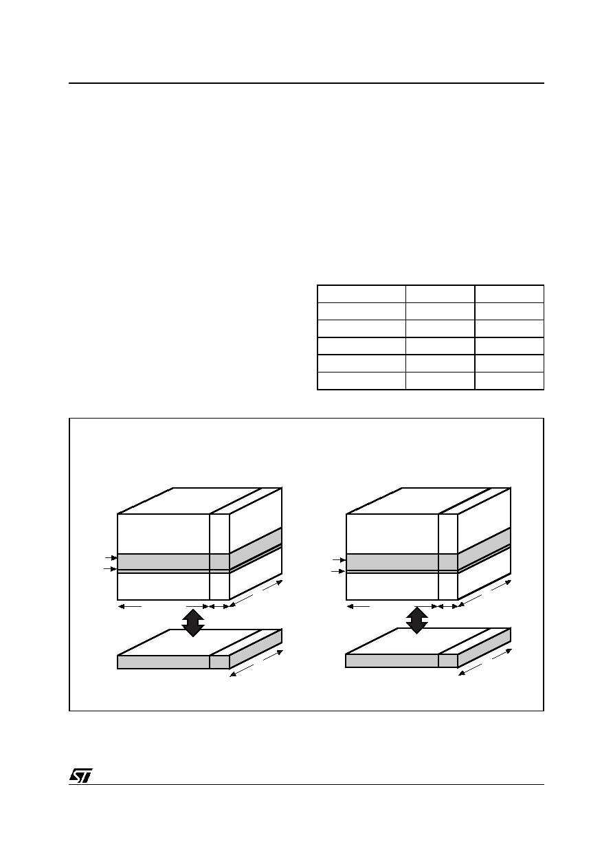
MEMORY ARRAY ORGANIZATION
The memory array is made up of NAND structures
where 32 cells are connected in series.
The memory array is organized in blocks where
each block contains 64 pages. The array is split
into two areas, the main area and the spare area.
The main area of the array is used to store data
whereas the spare area is typically used to store
Error correction Codes, software flags or Bad
Block identification.
In x8 devices the pages are split into a 2048 Byte
main area and a spare area of 64 Bytes. In the x16
devices the pages are split into a 1,024 Word main
area and a 32 Word spare area. Refer to Figure
Bad Blocks
The NAND Flash 2112 Byte/ 1056 Word Page de-
vices may contain Bad Blocks, that is blocks that
contain one or more invalid bits whose reliability is
not guaranteed. Additional Bad Blocks may devel-
op during the lifetime of the device.
The Bad Block Information is written prior to ship-
ping (refer to Bad Block Management section for
more details).
Table 4. shows the minimum number of valid
blocks in each device. The values shown include
both the Bad Blocks that are present when the de-
vice is shipped and the Bad Blocks that could de-
velop later on.
These blocks need to be managed using Bad
Blocks Management, Block Replacement or Error
Correction Codes (refer to SOFTWARE ALGO-
RITHMS section).
Table 4. Valid Blocks
Figure 8. Memory Array Organization
Density of Device
Min
Max
8 Gbits
8032
8192
4 Gbits
4016
4096
2 Gbits
2008
2048
1Gbit
1004
1024
512 Mbits
502
512
AI09854
Block = 64 Pages
Page = 2112 Bytes (2,048 + 64)
2,048 Bytes
2048 Bytes
Spare
Area
64
Bytes
Block
8 bits
64
Bytes
8 bits
Page
Page Buffer, 2112 Bytes
Block = 64 Pages
Page = 1056 Words (1024 + 32)
1,024 Words
1024 Words
Spare
Area
Main Area
32
Words
16 bits
32
Words
16 bits
Page Buffer, 1056 Words
Block
Page
x8 DEVICES
x16 DEVICES
Main Area
相关PDF资料 |
PDF描述 |
|---|---|
| NAND08GW3B3AZB6 | 1G X 8 FLASH 3V PROM, 25000 ns, PBGA63 |
| NAND256R3A1BN1F | 32M X 8 FLASH 1.8V PROM, 15000 ns, PDSO48 |
| NAND256R3A3BZA6F | 32M X 8 FLASH 1.8V PROM, 15000 ns, PBGA63 |
| NAND256R3A3CN1E | 32M X 8 FLASH 1.8V PROM, 15000 ns, PDSO48 |
| NAND256R4A1DN1E | 16M X 16 FLASH 1.8V PROM, 15000 ns, PDSO48 |
相关代理商/技术参数 |
参数描述 |
|---|---|
| NAND08GW3B4BN6E | 制造商:Micron Technology Inc 功能描述:NAND - Trays |
| NAND08GW3B4BN6F | 制造商:Micron Technology Inc 功能描述:NAND - Tape and Reel |
| NAND08GW3B4CN1F | 制造商:Micron Technology Inc 功能描述:NAND - Trays |
| NAND08GW3B4CZL6E | 制造商:Micron Technology Inc 功能描述:NAND - Trays |
| NAND08GW3C2AE01 | 功能描述:闪存 NAND & S.MEDIA FLASH RoHS:否 制造商:ON Semiconductor 数据总线宽度:1 bit 存储类型:Flash 存储容量:2 MB 结构:256 K x 8 定时类型: 接口类型:SPI 访问时间: 电源电压-最大:3.6 V 电源电压-最小:2.3 V 最大工作电流:15 mA 工作温度:- 40 C to + 85 C 安装风格:SMD/SMT 封装 / 箱体: 封装:Reel |
发布紧急采购,3分钟左右您将得到回复。