- 您现在的位置:买卖IC网 > PDF目录189002 > NAND512R3B3BZA6E (STMICROELECTRONICS) 64M X 8 FLASH 1.8V PROM, 35 ns, PBGA63 PDF资料下载
参数资料
| 型号: | NAND512R3B3BZA6E |
| 厂商: | STMICROELECTRONICS |
| 元件分类: | PROM |
| 英文描述: | 64M X 8 FLASH 1.8V PROM, 35 ns, PBGA63 |
| 封装: | 9.50 X 12 MM, 1 MM HEIGHT, 0.80 MM PITCH, ROHS COMPLIANT, VFBGA-63 |
| 文件页数: | 27/59页 |
| 文件大小: | 998K |
| 代理商: | NAND512R3B3BZA6E |
第1页第2页第3页第4页第5页第6页第7页第8页第9页第10页第11页第12页第13页第14页第15页第16页第17页第18页第19页第20页第21页第22页第23页第24页第25页第26页当前第27页第28页第29页第30页第31页第32页第33页第34页第35页第36页第37页第38页第39页第40页第41页第42页第43页第44页第45页第46页第47页第48页第49页第50页第51页第52页第53页第54页第55页第56页第57页第58页第59页
33/59
NAND512-B, NAND01G-B, NAND02G-B, NAND04G-B, NAND08G-B
DATA PROTECTION
The device has both hardware and software fea-
tures to protect against program and erase opera-
tions.
It features a Write Protect, WP, pin, which can be
used to protect the device against program and
erase operations. It is recommended to keep WP
at VIL during power-up and power-down.
In addition, to protect the memory from any invol-
untary program/erase operations during power-
transitions, the device has an internal voltage de-
tector which disables all functions whenever VCC
is below 1.5V.
The device features a Block Lock mode, which is
enabled by setting the Power-Up Read Enable,
Lock/Unlock Enable, PRL, signal to High.
The Block Lock mode has two levels of software
protection.
■
Blocks Lock/Unlock
■
Blocks Lock-down
Refer to Figure 21. for an overview of the protec-
tion mechanism.
Blocks Lock
All the blocks are locked simultaneously by issuing
a Blocks Lock command (see Table 10.).
All blocks are locked after power-up and when the
Write Protect signal is Low.
Once all the blocks are locked, one sequence of
consecutive blocks can be unlocked by using the
Blocks Unlock command.
Refer to Figure 25., Command Latch AC Wave-
forms for details on how to issue the command.
Blocks Unlock
A sequence of consecutive locked blocks can be
unlocked, to allow program or erase operations, by
issuing an Blocks Unlock command (see Table
The Blocks Unlock command consists of four
steps:
■
One bus cycle to setup the command
■
two or three bus cycles to give the Start Block
■
one bus cycle to confirm the command
■
two or three bus cycles to give the End Block
The Start Block Address must be nearer the logi-
cal LSB (Least Significant Bit) than End Block Ad-
dress.
If the Start Block Address is the same as the End
Block Address, only one block is unlocked.
Only one consecutive area of blocks can be un-
locked at any one time. It is not possible to unlock
multiple areas.
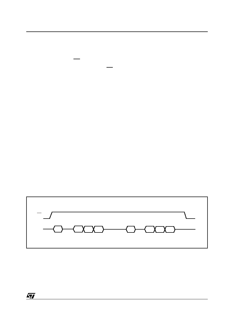
Figure 19. Blocks Unlock Operation
Note: Three address cycles are required for 2,4 and 8 Gb devices. The 512Mb and 1Gb devices only require two address cycles.
I/O
WP
Start Block Address, 3 cycles
ai08670
23h
Blocks Unlock
Command
Add1
Add2
Add3
24h
Add1
Add2
Add3
End Block Address, 3 cycles
相关PDF资料 |
PDF描述 |
|---|---|
| NAND512W3B3BN6E | 64M X 8 FLASH 3V PROM, 35 ns, PDSO48 |
| NAND512W3B3BZA6E | 64M X 8 FLASH 3V PROM, 35 ns, PBGA63 |
| NAND512W3B3AN1 | 64M X 8 FLASH 3V PROM, 35 ns, PDSO48 |
| NAND512W3B3BN1F | 64M X 8 FLASH 3V PROM, 35 ns, PDSO48 |
| NAND04GR4B3AN1 | 256M X 16 FLASH 1.8V PROM, 35 ns, PDSO48 |
相关代理商/技术参数 |
参数描述 |
|---|---|
| NAND512R4A2CWFD | 制造商:Micron Technology Inc 功能描述:NAND - Gel-pak, waffle pack, wafer, diced wafer on film |
| NAND512R4A2CZA6 | 制造商:Micron Technology Inc 功能描述:512MB. 3V X8 NO OPTION TSOP48TSOP-1 48 12X20 AL 42 - Trays |
| NAND512R4A2DDI6 | 制造商:Micron Technology Inc 功能描述:NAND - Gel-pak, waffle pack, wafer, diced wafer on film |
| NAND512W3A0AN6 | 功能描述:闪存 NAND & S.MEDIA FLASH RoHS:否 制造商:ON Semiconductor 数据总线宽度:1 bit 存储类型:Flash 存储容量:2 MB 结构:256 K x 8 定时类型: 接口类型:SPI 访问时间: 电源电压-最大:3.6 V 电源电压-最小:2.3 V 最大工作电流:15 mA 工作温度:- 40 C to + 85 C 安装风格:SMD/SMT 封装 / 箱体: 封装:Reel |
| NAND512W3A0AN6E | 功能描述:闪存 2.7-3.6V 512M(64Mx8) RoHS:否 制造商:ON Semiconductor 数据总线宽度:1 bit 存储类型:Flash 存储容量:2 MB 结构:256 K x 8 定时类型: 接口类型:SPI 访问时间: 电源电压-最大:3.6 V 电源电压-最小:2.3 V 最大工作电流:15 mA 工作温度:- 40 C to + 85 C 安装风格:SMD/SMT 封装 / 箱体: 封装:Reel |
发布紧急采购,3分钟左右您将得到回复。