- 您现在的位置:买卖IC网 > PDF目录189002 > NAND512R3B3BZA6E (STMICROELECTRONICS) 64M X 8 FLASH 1.8V PROM, 35 ns, PBGA63 PDF资料下载
参数资料
| 型号: | NAND512R3B3BZA6E |
| 厂商: | STMICROELECTRONICS |
| 元件分类: | PROM |
| 英文描述: | 64M X 8 FLASH 1.8V PROM, 35 ns, PBGA63 |
| 封装: | 9.50 X 12 MM, 1 MM HEIGHT, 0.80 MM PITCH, ROHS COMPLIANT, VFBGA-63 |
| 文件页数: | 31/59页 |
| 文件大小: | 998K |
| 代理商: | NAND512R3B3BZA6E |
第1页第2页第3页第4页第5页第6页第7页第8页第9页第10页第11页第12页第13页第14页第15页第16页第17页第18页第19页第20页第21页第22页第23页第24页第25页第26页第27页第28页第29页第30页当前第31页第32页第33页第34页第35页第36页第37页第38页第39页第40页第41页第42页第43页第44页第45页第46页第47页第48页第49页第50页第51页第52页第53页第54页第55页第56页第57页第58页第59页
37/59
NAND512-B, NAND01G-B, NAND02G-B, NAND04G-B, NAND08G-B
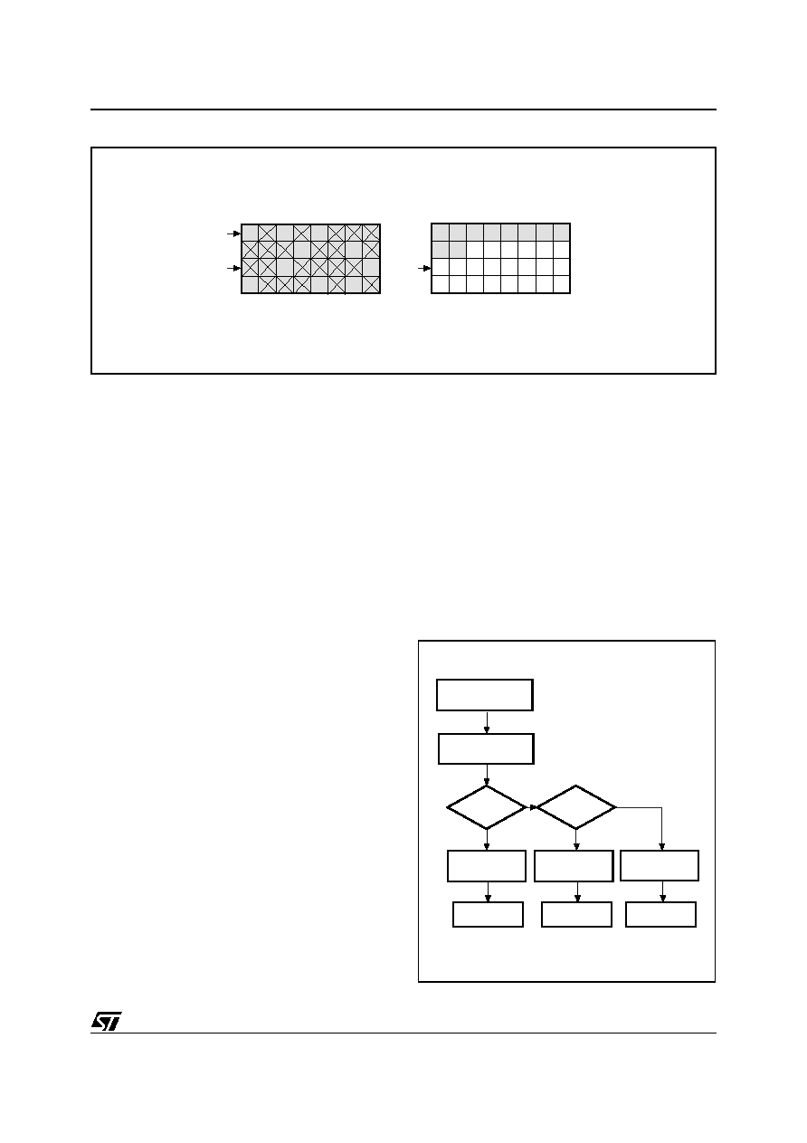
Figure 23. Garbage Collection
Garbage Collection
When a data page needs to be modified, it is faster
to write to the first available page, and the previous
page is marked as invalid. After several updates it
is necessary to remove invalid pages to free some
memory space.
To free this memory space and allow further pro-
gram operations it is recommended to implement
a Garbage Collection algorithm. In a Garbage Col-
lection software the valid pages are copied into a
free area and the block containing the invalid pag-
es is erased (see Figure 23.).
Wear-leveling Algorithm
For write-intensive applications, it is recommend-
ed to implement a Wear-leveling Algorithm to
monitor and spread the number of write cycles per
block.
In memories that do not use a Wear-Leveling Al-
gorithm not all blocks get used at the same rate.
Blocks with long-lived data do not endure as many
write cycles as the blocks with frequently-changed
data.
The Wear-leveling Algorithm ensures that equal
use is made of all the available write cycles for
each block. There are two wear-leveling levels:
■
First Level Wear-leveling, new data is
programmed to the free blocks that have had
the fewest write cycles
■
Second Level Wear-leveling, long-lived data is
copied to another block so that the original
block can be used for more frequently-
changed data.
The Second Level Wear-leveling is triggered when
the difference between the maximum and the min-
imum number of write cycles per block reaches a
specific threshold.
Error Correction Code
An Error Correction Code (ECC) can be imple-
mented in the Nand Flash memories to identify
and correct errors in the data.
For every 2048 bits in the device it is recommend-
ed to implement 22 bits of ECC (16 bits for line par-
ity plus 6 bits for column parity).
An ECC model is available in VHDL or Verilog.
Contact the nearest ST Microelectronics sales of-
fice for more details.
Figure 24. Error Detection
Valid
Page
Invalid
Page
Free
Page
(Erased)
Old Area
AI07599B
New Area (After GC)
New ECC generated
during read
XOR previous ECC
with new ECC
All results
= zero?
22 bit data = 0
YES
11 bit data = 1
NO
1 bit data = 1
Correctable
Error
ECC Error
No Error
ai08332
>1 bit
= zero?
YES
NO
相关PDF资料 |
PDF描述 |
|---|---|
| NAND512W3B3BN6E | 64M X 8 FLASH 3V PROM, 35 ns, PDSO48 |
| NAND512W3B3BZA6E | 64M X 8 FLASH 3V PROM, 35 ns, PBGA63 |
| NAND512W3B3AN1 | 64M X 8 FLASH 3V PROM, 35 ns, PDSO48 |
| NAND512W3B3BN1F | 64M X 8 FLASH 3V PROM, 35 ns, PDSO48 |
| NAND04GR4B3AN1 | 256M X 16 FLASH 1.8V PROM, 35 ns, PDSO48 |
相关代理商/技术参数 |
参数描述 |
|---|---|
| NAND512R4A2CWFD | 制造商:Micron Technology Inc 功能描述:NAND - Gel-pak, waffle pack, wafer, diced wafer on film |
| NAND512R4A2CZA6 | 制造商:Micron Technology Inc 功能描述:512MB. 3V X8 NO OPTION TSOP48TSOP-1 48 12X20 AL 42 - Trays |
| NAND512R4A2DDI6 | 制造商:Micron Technology Inc 功能描述:NAND - Gel-pak, waffle pack, wafer, diced wafer on film |
| NAND512W3A0AN6 | 功能描述:闪存 NAND & S.MEDIA FLASH RoHS:否 制造商:ON Semiconductor 数据总线宽度:1 bit 存储类型:Flash 存储容量:2 MB 结构:256 K x 8 定时类型: 接口类型:SPI 访问时间: 电源电压-最大:3.6 V 电源电压-最小:2.3 V 最大工作电流:15 mA 工作温度:- 40 C to + 85 C 安装风格:SMD/SMT 封装 / 箱体: 封装:Reel |
| NAND512W3A0AN6E | 功能描述:闪存 2.7-3.6V 512M(64Mx8) RoHS:否 制造商:ON Semiconductor 数据总线宽度:1 bit 存储类型:Flash 存储容量:2 MB 结构:256 K x 8 定时类型: 接口类型:SPI 访问时间: 电源电压-最大:3.6 V 电源电压-最小:2.3 V 最大工作电流:15 mA 工作温度:- 40 C to + 85 C 安装风格:SMD/SMT 封装 / 箱体: 封装:Reel |
发布紧急采购,3分钟左右您将得到回复。