- 您现在的位置:买卖IC网 > PDF目录16746 > NCN6001DTBEVB (ON Semiconductor)EVAL BOARD FOR NCN6001DTB PDF资料下载
参数资料
| 型号: | NCN6001DTBEVB |
| 厂商: | ON Semiconductor |
| 文件页数: | 19/36页 |
| 文件大小: | 0K |
| 描述: | EVAL BOARD FOR NCN6001DTB |
| 设计资源: | NCN6001DTBEVB Gerber Files NCN6001 Demo Brd Schematic NCN6001DBEVB BOM |
| 标准包装: | 1 |
| 主要目的: | 接口,智能卡 |
| 嵌入式: | 是,MCU,8 位 |
| 已用 IC / 零件: | NCN6001 |
| 主要属性: | 与 ISO 7816-3,EMV,GIE-CB 兼容 |
| 次要属性: | 符合 GSM 规定 |
| 已供物品: | 板 |
| 其它名称: | NCN6001DTBEVBOS |
第1页第2页第3页第4页第5页第6页第7页第8页第9页第10页第11页第12页第13页第14页第15页第16页第17页第18页当前第19页第20页第21页第22页第23页第24页第25页第26页第27页第28页第29页第30页第31页第32页第33页第34页第35页第36页
NCN6001
http://onsemi.com
26
SMART CARD CLOCK DIVIDER
The main purpose of the builtin clock generator is
threefold:
1. Adapts the voltage level shifter to cope with the
different voltages that might exist between the
MPU and the Smart Card.
2. Provides a frequency division to adapt the Smart
Card operating frequency from the external clock
source.
3. Controls the clock state according to the smart
card specification.
In addition, the NCN6001 adjusts the signal coming from
the microprocessor to get the Duty Cycle window as defined
by the ISO78163 specification.
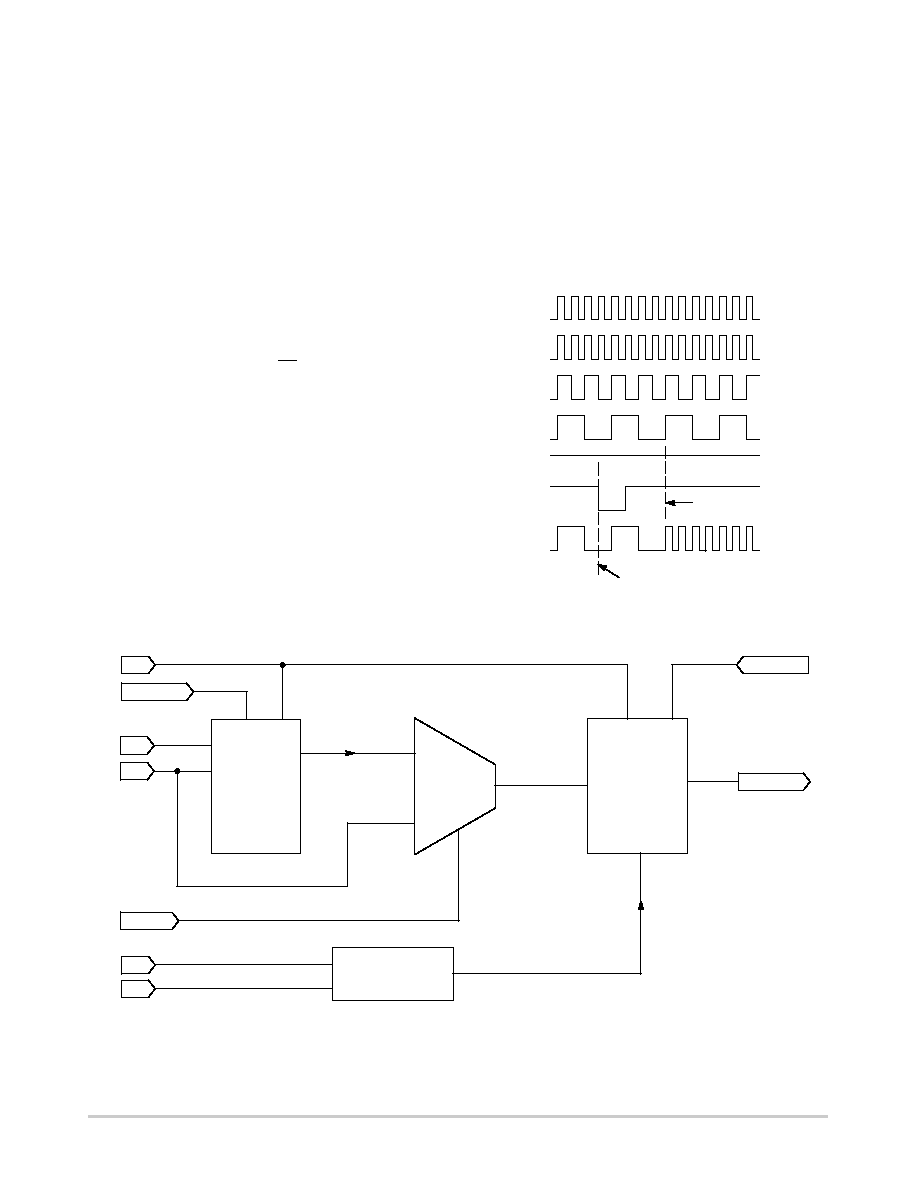
The byte content of the SPI port, B2 & B3, fulfills the
programming functions when CS is Low as depicted in
can handle a 20 MHz frequency maximum signal, the
divider being capable to provide a 1:4 ratio. Of course, the
ratio must be defined by the engineer to cope with the Smart
Card considered in a given application and, in any case, the
output clock [CRD_CLK] shall be limited to 20 MHz
maximum. In order to minimize the dI/dt and dV/dV
developed in the CRD_CLK line, the output stage includes
a special function to adapt the slope of the clock signal for
different applications. This function is programmed by the
MOSI register (Table 2: WRT_REG Bits Definitions and
Functions) whatever be the clock division.
In order to avoid any duty cycle out of the smart card
ISO78163 specification, the divider is synchronized by the
last flip flop, thus yielding a constant 50% duty cycle,
whatever be the divider ratio (Figure 25). Consequently, the
output CRD_CLK frequency division can be delayed by
four CLK_IN pulses and the microcontroller software must
take this delay into account prior to launch a new data
transaction. On the other hand, the output signal Duty Cycle
cannot be guaranteed 50% if the division ratio is 1 and if the
input Duty Cycle signal is not within the 46–56% range.
The input signals CLK_IN and MOSI/b3 are
automatically routed to the level shifter and control block
according to the mode of operation.
CRD_CLK
CLOCK_IN
CLOCK : 2
CLOCK : 4
B2
B3
Clock is updated upon
These bits program
Internal
CLOCK programming is activated
by the B2 + B3 logic state
CLOCK = 1:1 ratio
CLOCK : 1
Figure 25. Typical Clock Divider Synchronization
CLOCK: 4 rising edge
CLOCK
Divider
Figure 26. Basic Clock Divider and Level Shifter
B1
B0
B3
B2
CLK_IN
VCC
CRD_CLK
CRD_VCC
LEVEL SHIFTER
AND CONTROL
Programming
CRD_CLK Slope
NOTE: Bits [B0...B3] come from SPI data
Programming
CRD_CLK
Division
SYNC
ASYNC
SYNC
U1
DIGITAL_MUX
OUT
SEL
A
B
相关PDF资料 |
PDF描述 |
|---|---|
| 2474-12L | INDUCTOR 8.2UH POWER AXIAL |
| 0982661043 | CBL 33POS 0.5MM JMPR TYPE A 7" |
| UWT0G470MCL1GB | CAP ALUM 47UF 4V 20% SMD |
| V48C5C100B | CONVERTER MOD DC/DC 5V 100W |
| H3AAH-2406M | IDC CABLE - HSC24H/AE24M/HSC24H |
相关代理商/技术参数 |
参数描述 |
|---|---|
| NCN6001DTBR2 | 功能描述:输入/输出控制器接口集成电路 2.7V POS/ATM Smart RoHS:否 制造商:Silicon Labs 产品: 输入/输出端数量: 工作电源电压: 最大工作温度:+ 85 C 最小工作温度:- 40 C 安装风格:SMD/SMT 封装 / 箱体:QFN-64 封装:Tray |
| NCN6001DTBR2G | 功能描述:输入/输出控制器接口集成电路 2.7V POS/ATM Smart Card Interface RoHS:否 制造商:Silicon Labs 产品: 输入/输出端数量: 工作电源电压: 最大工作温度:+ 85 C 最小工作温度:- 40 C 安装风格:SMD/SMT 封装 / 箱体:QFN-64 封装:Tray |
| NCN6001MUTWG | 制造商:ON Semiconductor 功能描述:ANA COMPACT SMARTCARD IC - Tape and Reel 制造商:ON Semiconductor 功能描述:IC INTERFACE SMART CARD 制造商:ON Semiconductor 功能描述:REEL - ANA COMPACT SMARTCARD IC |
| NCN6004A | 制造商:ONSEMI 制造商全称:ON Semiconductor 功能描述:Dual SAM/SIM Interface Integrated Circuit |
| NCN6004A/D | 制造商:ONSEMI 制造商全称:ON Semiconductor 功能描述:Dual SAM/SIM Interface Integrated Circuit |
发布紧急采购,3分钟左右您将得到回复。