- 您现在的位置:买卖IC网 > PDF目录22101 > NCP1027P065G (ON Semiconductor)IC SWIT PWM PROG CM OVP HV 8DIP PDF资料下载
参数资料
| 型号: | NCP1027P065G |
| 厂商: | ON Semiconductor |
| 文件页数: | 19/30页 |
| 文件大小: | 0K |
| 描述: | IC SWIT PWM PROG CM OVP HV 8DIP |
| 标准包装: | 1,000 |
| 输出隔离: | 隔离 |
| 频率范围: | 58.5kHz ~ 71.5kHz |
| 输入电压: | 7.9 V ~ 10 V |
| 输出电压: | 700V |
| 功率(瓦特): | 25W |
| 工作温度: | 0°C ~ 125°C |
| 封装/外壳: | 8-DIP(0.300",7.62mm),7 引线 |
| 供应商设备封装: | 8-PDIP |
| 包装: | 管件 |
| 其它名称: | NCP1027P065GOS |
第1页第2页第3页第4页第5页第6页第7页第8页第9页第10页第11页第12页第13页第14页第15页第16页第17页第18页当前第19页第20页第21页第22页第23页第24页第25页第26页第27页第28页第29页第30页
�� �
�
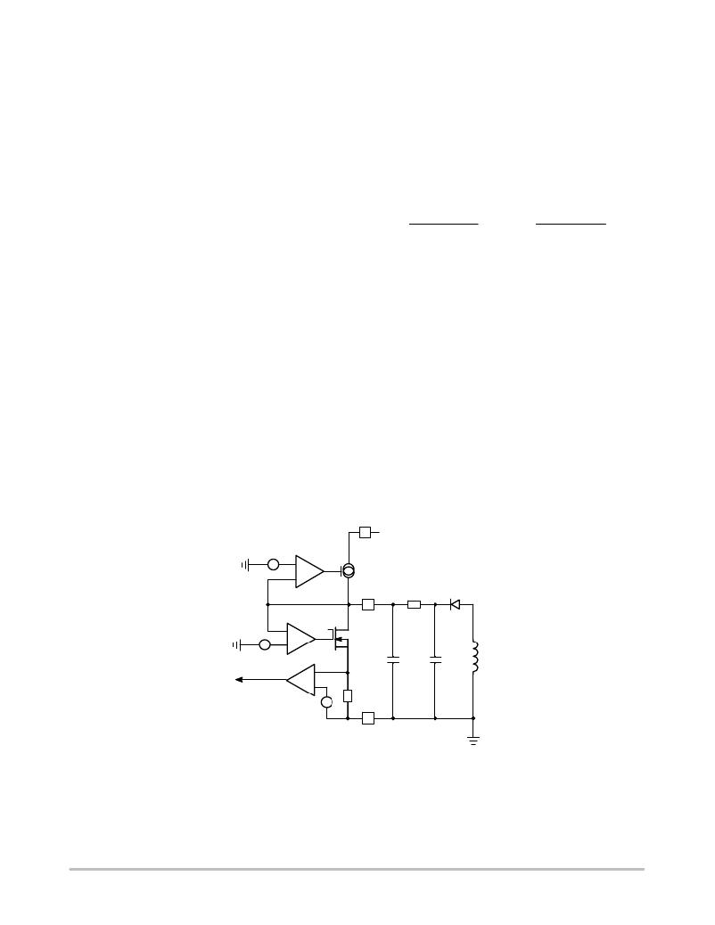
�NCP1027�
�Auto-Recovery� Overvoltage� Protection�
�The� particular� NCP1027� arrangement� offers� a� simple�
�way� to� prevent� output� voltage� runaway� when� the�
�optocoupler� fails.� As� Figure� 34� shows,� an� active� Zener�
�diode� monitors� and� protects� the� V� CC� pin.� Below� its�
�equivalent� breakdown� voltage,� that� is� to� say� 8.7� V� typical,�
�no� current� flows� in� it.� If� the� auxiliary� V� CC� pushes� too� much�
�current� inside� the� Zener,� then� the� controller� considers� an�
�OVP� situation� and� stops� the� pulses.� Figure� 34� shows� that�
�the� insertion� of� a� resistor� (� R� limit� )� between� the� auxiliary� DC�
�standby� (output� unloaded).� Thus,� care� must� be� taken� when�
�calculating� R� limit� 1)� to� not� trigger� the� V� CC� overcurrent� latch�
�(by� injecting� 6.0� mA� into� the� active� clamp� –� always� use� the�
�minimum� value� for� worse� case� design)� in� normal� operation�
�but� 2)� not� to� drop� too� much� voltage� over� R� limit� when�
�entering� standby.� Otherwise,� the� converter� will� enter� burst�
�mode� as� it� will� sense� an� UVLO� condition.� Based� on� these�
�recommendations,� we� are� able� to� bound� R� limit� between� two�
�equations:�
�level� and� the� V� CC� pin� is� mandatory� a)� not� to� damage� the�
�internal� 8.7� V� Zener� diode� during� an� overshoot� for� instance�
�(absolute� maximum� current� is� 15� mA)� b)� to� implement� the�
�Vnom- Vclamp�
�Itrip�
�v� Rlimit� v�
�Vstby- VCCON�
�ICC1�
�(eq.� 3)�
�fail-safe� optocoupler� protection� (OVP)� as� offered� by� the�
�active� clamp.� Please� note� that� there� cannot� be� bad�
�interaction� between� the� clamping� voltage� of� the� internal�
�Zener� and� VCC� ON� since� this� clamping� voltage� is� actually�
�built� on� top� of� VCC� ON� with� a� fixed� amount� of� offset�
�(200� mV� typical).� R� limit� should� be� carefully� selected� to�
�avoid� triggering� the� OVP� as� we� discussed,� but� also� to� avoid�
�disturbing� the� V� CC� in� low/light� load� conditions.� The�
�following� details� how� to� evaluate� the� R� limit� value.�
�Self-supplying� controllers� in� extremely� low� standby�
�applications� often� puzzles� the� designer.� Actually,� if� an�
�SMPS� operated� at� nominal� load� can� deliver� an� auxiliary�
�voltage� of� an� arbitrary� 16� V� (V� nom� ),� this� voltage� can� drop�
�below� 10� V� (V� stby� )� when� entering� standby.� This� is� because�
�the� recurrence� of� the� switching� pulses� expands� so� much,�
�that� the� low� frequency� refueling� rate� of� the� V� CC� capacitor�
�is� not� enough� to� keep� a� proper� auxiliary� voltage.� Figure� 35�
�portrays� a� typical� scope� shot� of� an� SMPS� entering� deep�
�Where:�
�V� nom� is� the� auxiliary� voltage� at� nominal� load.�
�V� stdby� is� the� auxiliary� voltage� when� standby� is� entered.�
�I� trip� is� the� current� corresponding� to� the� nominal� operation.�
�It� thus� must� be� selected� to� avoid� false� tripping� in� overshoot�
�conditions.� Always� use� the� minimum� of� the� specification�
�for� a� robust� design.�
�ICC1� is� the� controller� consumption.� This� number� slightly�
�decreases� compared� to� ICC1� from� the� spec� since� the� part�
�in� standby� does� almost� not� switch.� It� is� around� 1.0� mA� for�
�the� 65� kHz� version.�
�VCC� (min)� is� the� level� above� which� the� auxiliary� voltage�
�must� be� maintained� to� keep� the� controller� away� from� the�
�UVLO� trip� point.� It� is� good� to� obtain� around� 8.0� V� in� order�
�to� offer� an� adequate� design� margin,� e.g.� to� not� reactivate� the�
�startup� source� (which� is� not� a� problem� in� itself� if� low�
�standby� power� does� not� matter).�
�Drain�
�V� CCON� =� 8.5� V�
�V� CC(min)� =� 7.5� V�
�+�
�-�
�+�
�Startup�
�Source�
�+�
�V� CC�
�R� limit�
�D1�
�-�
�+�
�V� clamp� =� 8.7� V� Typ.�
�+�
�C� VCC�
�+�
�C� AUX�
�L� aux�
�Latch�
�+�
�-�
�+�
�I� >� 6� mA�
�Ground�
�Figure� 34.� A� more� detailed� view� of� the� NCP1027� offers� better�
�insight� on� how� to� properly� wire� an� auxiliary� winding.�
�Since� R� limit� shall� not� bother� the� controller� in� standby,� e.g.�
�keep� Vauxiliary� to� around� 8.0� V� (as� selected� above),� we�
�purposely� select� a� Vnom� well� above� this� value.� As�
�explained� before,� experience� shows� that� a� 40%� decrease�
�can� be� seen� on� auxiliary� windings� from� nominal� operation�
�down� to� standby� mode.� Let's� select� a� nominal� auxiliary�
�winding� of� 20� V� to� offer� sufficient� margin� regarding� 8.0� V�
�when� in� standby� (� R� limit� also� drops� voltage� in� standby� …� ).�
�http://onsemi.com�
�19�
�相关PDF资料 |
PDF描述 |
|---|---|
| ISL61851LIBZ-T | IC USB PWR CTRLR DUAL 8SOIC |
| AP130-20WL-7 | IC REG LDO 2V .3A SC59-3 |
| S1BB-13-F | RECTIFIER GPP 100V 1A SMD |
| TAP155M025CCS | CAP TANT 1.5UF 25V 20% RADIAL |
| VI-23N-EV-F1 | CONVERTER MOD DC/DC 18.5V 150W |
相关代理商/技术参数 |
参数描述 |
|---|---|
| NCP1027P100G | 功能描述:交流/直流开关转换器 PWM Current Mode Controller RoHS:否 制造商:STMicroelectronics 输出电压:800 V 输入/电源电压(最大值):23.5 V 输入/电源电压(最小值):11.5 V 开关频率:115 kHz 电源电流:1.6 mA 工作温度范围:- 40 C to + 150 C 安装风格:SMD/SMT 封装 / 箱体:SSO-10 封装:Reel |
| NCP1027PO65G | 制造商:Rochester Electronics LLC 功能描述:- Bulk 制造商:ON Semiconductor 功能描述: |
| NCP1028 | 制造商:ONSEMI 制造商全称:ON Semiconductor 功能描述:Power Factor Controllers |
| NCP1028LEDGEVB | 功能描述:电源管理IC开发工具 720MA 18V LED DRIVER RoHS:否 制造商:Maxim Integrated 产品:Evaluation Kits 类型:Battery Management 工具用于评估:MAX17710GB 输入电压: 输出电压:1.8 V |
| NCP1028P065G | 功能描述:电流型 PWM 控制器 NCP1028 65 KHZ RoHS:否 制造商:Texas Instruments 开关频率:27 KHz 上升时间: 下降时间: 工作电源电压:6 V to 15 V 工作电源电流:1.5 mA 输出端数量:1 最大工作温度:+ 105 C 安装风格:SMD/SMT 封装 / 箱体:TSSOP-14 |
发布紧急采购,3分钟左右您将得到回复。