参数资料
| 型号: | NCP1650EVB |
| 厂商: | ON Semiconductor |
| 文件页数: | 15/31页 |
| 文件大小: | 0K |
| 描述: | BOARD EVAL NCP1650 PFC CTLR |
| 设计资源: | NCP1650EVB Schematic NCP1650EVB Bill of Materials NCP1650EVB Test Procedure NCP1650EVB Gerber Zip |
| 标准包装: | 1 |
| 主要目的: | 电源管理,功率因数校正 |
| 嵌入式: | 否 |
| 已用 IC / 零件: | NCP1650 |
| 已供物品: | 板 |
| 其它名称: | NCP1650EVB-ND NCP1650EVBOS |
第1页第2页第3页第4页第5页第6页第7页第8页第9页第10页第11页第12页第13页第14页当前第15页第16页第17页第18页第19页第20页第21页第22页第23页第24页第25页第26页第27页第28页第29页第30页第31页
�� �
�
�NCP1650�
�+Bus�
�FB/SD�
�--�
�V� error(dc)�
�LOOP�
�COMP�
�4V�
�+�
�VOLTAGE�
�ERROR�
�AMP�
�4V�
�--�
�PWM�
�DRIVER�
�DRIVE�
�R� ac1�
�+�
�PWM�
�Logic�
�1�
�R� ac2�
�AC� INPUT�
�+�
�--�
�REFERENCE�
�MULTIPLIER�
�V� line�
�.75�
�V� ref�
�AC� ERROR�
�AMP�
�+�
�--�
�V� error(ac)�
�V� error(ac)� ?�
�V� error(ac)�
�V--I�
�AC�
�REFERENCE� k� ?� I� in�
�BUFFER�
�CURRENT�
�SENSE�
�AMPLIFIER�
�I� S--�
�AVERAGE� CURRENT�
�COMPENSATION�
�REF� FILTER�
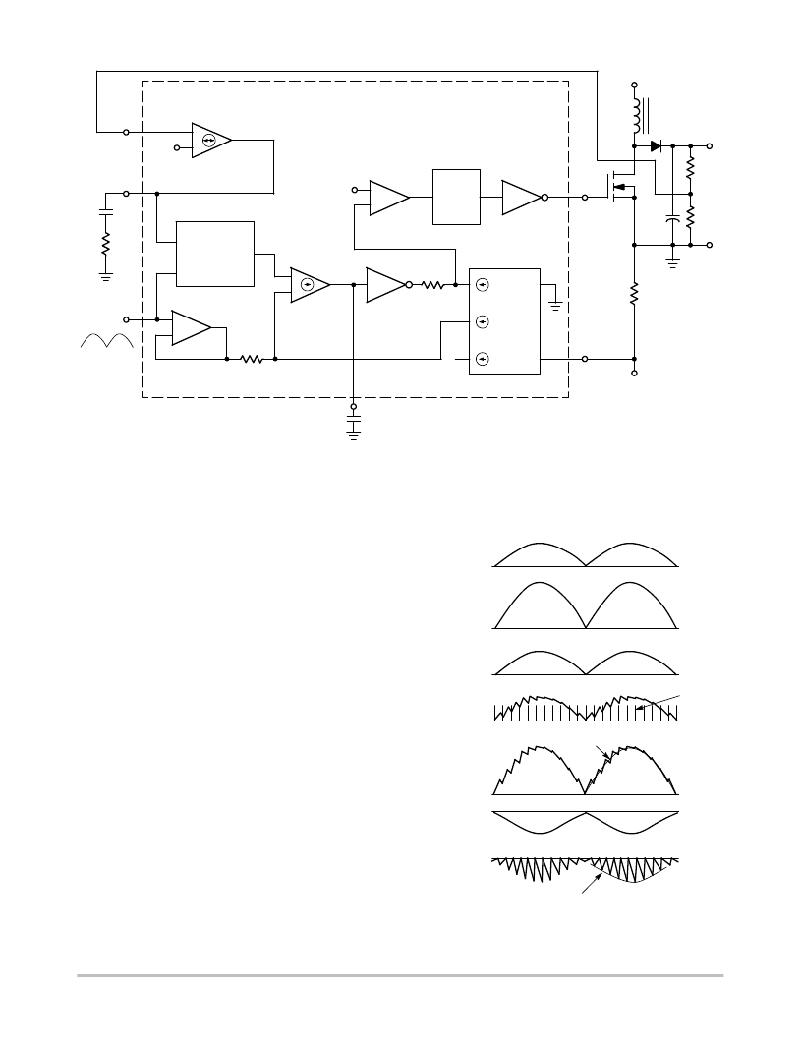
�Figure� 32.� Simplified� Block� Diagram� of� Basic� PFC� Control� Circuit�
�--Bus�
�The� key� to� understanding� how� the� input� current� is� shaped�
�into� a� high� quality� sine� wave� is� the� operation� of� the� AC� error�
�amplifier.� The� inputs� of� an� operational� amplifier� operating�
�in� its� linear� range,� must� be� equal.�
�There� are� several� secondary� effects,� that� create� small�
�differences� between� the� inverting� and� non--inverting� inputs,�
�but� for� the� purpose� of� this� analysis� they� can� be� considered� to�
�be� equal.�
�The� fullwave� rectified� sinewave� output� of� the� reference�
�multiplier� is� fed� into� the� non--inverting� input� of� the� AC� error�
�amplifier.� The� inverting� input� to� the� AC� error� amplifier�
�receives� a� signal� that� is� comprised� of� the� input� fullwave�
�rectified� sinewave� (which� is� not� modified� by� the� reference�
�output� so� that� the� signal� can� be� summed� with� the�
�instantaneous� input� switching� current� (I� in� ).� The� output� of� the�
�buffer� is� still� V� errorac� .�
�AC� Input�
�V� ref�
�V� line�
�multiplier),� and� summed� with� the� filtered� input� current.�
�Since� the� two� inputs� to� this� amplifier� will� be� at� the� same�
�potential,� the� complex� signal� at� the� inverting� input� will� have�
�k� ?� I� in�
�OSC�
�the� same� wave� shape� as� the� AC� reference� signal.� The� AC�
�reference� signal� (V� ref� )� is� a� fullwave� rectified� sinewave,� and�
�the� AC� input� signal� (V� line� )� is� also� a� fullwave� rectified�
�sinewave,� therefore,� the� AC� current� signal� (I� in� ),� must� also� be�
�a� fullwave� rectified� sinewave.� This� relationship� gives� the�
�formula:�
�Vref� =� .75� ·� Vline� +� (k� ·� Iin)�
�The� I� in� signal� has� a� wide� bandwidth,� and� its� instantaneous�
�value� will� not� follow� the� low� frequency� fullwave� rectified�
�sinewave� exactly,� however,� the� output� of� the� AC� error�
�amplifier� has� a� low� frequency� pole� that� allows� the� average�
�V� line� +� k� ?� I� in�
�V� error(ac)�
�V� error(ac)� ?�
�V� ref�
�V� error(ac)�
�4� V� ref�
�GND�
�4� V� ref�
�GND�
�value� of� the� .75� V� line� +� (k� x� I� in� )� to� follow� V� ref� .� Since� the� AC�
�error� amplifier� is� a� transconductance� amplifier,� it� is� followed�
�by� an� inverting� unity� gain� buffer� stage� with� a� low� impedance�
�http://onsemi.com�
�15�
�Figure� 33.� Typical� Signals� for� PFC� Circuit�
�相关PDF资料 |
PDF描述 |
|---|---|
| NCP1652L48VGEVB | BOARD EVAL 100W 48V NCP1652 PFC |
| NCP1653EVB | BOARD EVAL FOR NCP1653 |
| NCP2993FCT2GEVB | BOARD EVAL NCP2993 AUDIO PWR AMP |
| NCP345SNT1G | IC DETECTOR OVER VOLTAGE 5TSOP |
| NCP346SN2T1G | IC DETECTOR OVER VOLTAGE 5TSOP |
相关代理商/技术参数 |
参数描述 |
|---|---|
| NCP1651DR2 | 功能描述:功率因数校正 IC Single Stage PFC RoHS:否 制造商:Fairchild Semiconductor 开关频率:300 KHz 最大功率耗散: 最大工作温度:+ 125 C 安装风格:SMD/SMT 封装 / 箱体:SOIC-8 封装:Reel |
| NCP1651DR2G | 功能描述:功率因数校正 IC Single Stage PFC RoHS:否 制造商:Fairchild Semiconductor 开关频率:300 KHz 最大功率耗散: 最大工作温度:+ 125 C 安装风格:SMD/SMT 封装 / 箱体:SOIC-8 封装:Reel |
| NCP1652ADR2G | 功能描述:功率因数校正 IC ANA PFC CONTROLLER RoHS:否 制造商:Fairchild Semiconductor 开关频率:300 KHz 最大功率耗散: 最大工作温度:+ 125 C 安装风格:SMD/SMT 封装 / 箱体:SOIC-8 封装:Reel |
| NCP1652DR2G | 功能描述:功率因数校正 IC ANA PFC CONTROLLER RoHS:否 制造商:Fairchild Semiconductor 开关频率:300 KHz 最大功率耗散: 最大工作温度:+ 125 C 安装风格:SMD/SMT 封装 / 箱体:SOIC-8 封装:Reel |
| NCP1652DWR2G | 功能描述:功率因数校正 IC ANA PFC CONTROLLER RoHS:否 制造商:Fairchild Semiconductor 开关频率:300 KHz 最大功率耗散: 最大工作温度:+ 125 C 安装风格:SMD/SMT 封装 / 箱体:SOIC-8 封装:Reel |
发布紧急采购,3分钟左右您将得到回复。