参数资料
| 型号: | NCP1650EVB |
| 厂商: | ON Semiconductor |
| 文件页数: | 18/31页 |
| 文件大小: | 0K |
| 描述: | BOARD EVAL NCP1650 PFC CTLR |
| 设计资源: | NCP1650EVB Schematic NCP1650EVB Bill of Materials NCP1650EVB Test Procedure NCP1650EVB Gerber Zip |
| 标准包装: | 1 |
| 主要目的: | 电源管理,功率因数校正 |
| 嵌入式: | 否 |
| 已用 IC / 零件: | NCP1650 |
| 已供物品: | 板 |
| 其它名称: | NCP1650EVB-ND NCP1650EVBOS |
第1页第2页第3页第4页第5页第6页第7页第8页第9页第10页第11页第12页第13页第14页第15页第16页第17页当前第18页第19页第20页第21页第22页第23页第24页第25页第26页第27页第28页第29页第30页第31页
�� �
�
�NCP1650�
�recommended� that� an� external� resistor� be� used� at� the� “Ref�
�Gain”� pin,� due� to� tolerance� variations� of� the� internal�
�resistances.�
�The� voltage--to--current� conversion� is� performed� in� the�
�Multiplier�
�Voltage/Power� ORing� network.� This� circuit� also� limits� the�
�maximum� input� signal� (from� the� error� amplifier)� to� 3� volts.�
�Power Multiplier/Current Sense Amplifier� There� is� no�
�voltage--to--current� converter� on� the� power� multiplier.� The�
�AC� Ref�
�1k�
�25� k�
�4.5� V�
�+�
�--�
�AC� Error�
�Amplifier�
�current� output� of� the� current� sense� amplifier� is� used� for� the�
�(3.)� V9� =�
�analog� input� with� no� scaling.�
�The� power� multiplier� requires� an� external� resistor� as� well�
�as� an� external� capacitor.� The� value� of� the� resistor� at� pin� 9�
�(max� power)� will� depend� on� the� value� of� the� resistor� used� at�
�pin� 10� for� the� current� gain� and� the� maximum� desired� output�
�power� of� the� converter.� These� resistors� should� be� the� same�
�style� of� resistor� and� have� the� same� temperature� coefficients�
�for� best� performance.�
�The� gain� of� the� power� multiplier� is� based� on� the� values� of�
�external� components� on� this� multiplier� as� well� as� the� current�
�sense� amplifier.� The� current� sense� amplifier� output� that�
�drives� the� power� multiplier� has� its� gain� controlled� by� R� 9� and�
�R� 10� ,� and� is� filtered� by� a� capacitor� on� pin� 11� which� removes�
�the� high� frequency� content� from� the� inductor� current� signal.�
�The� gain� for� the� power� multiplier� can� be� calculated� as�
�follows:�
�(1.)� V9� =� ICS� ×� R9� ×� (Vac� ∕� Vramp)�
�Where:�
�I� CS� is� the� rms� value� of� the� average� current� out� of� the� current�
�sense� amplifier�
�R� 9� is� the� resistor� value� at� pin� 9� (Ohms)�
�V� ac� is� the� rms� voltage� at� pin� 5�
�V� ramp� is� the� sawtooth� p--p� ramp� voltage� (4.0� volts)�
�and,�
�(2.)� ICS� =� VCS� ×� 15� ∕� R10�
�Since� the� pole� at� pin� 12� is� much� greater� than� twice� the� line�
�frequency� we� can� ignore� the� effects� of� the� capacitor� on� this�
�pin.� V� CS� is� the� differential� current� sense� rms� input� voltage.�
�Equations� 1� and� 2� can� be� rearranged� to� give� the� gain� of� the�
�multiplier:�
�3.75� ?� R9� ?� VCS� ?� Vac�
�R10�
�This� gain� equation� gives� the� output� voltage� of� the�
�multiplier,� where� the� inputs� are� the� AC� fullwave� rectified�
�sinewave� and� the� current� sense� input� signal.�
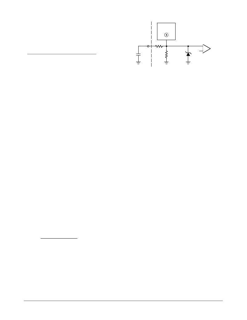
�Figure� 35.� Reference� Multiplier� Clamp� Circuit�
�There� is� a� 1� k� resistor� between� the� AC� Ref� pin� and� the� AC�
�Error� Amplifier� for� ESD� protection.� Due� to� this� resistor,� the�
�voltage� on� pin� 4� will� exceed� 4.5� volts� under� some� conditions,�
�but� the� maximum� voltage� at� the� non--inverting� AC� Error�
�Amplifier� input� will� be� clamped� at� 4.5� volts.�
�Feedback/Shutdown�
�The� FB/SD� pin� is� a� multiple� function� pin.� Its� primary�
�function� is� to� provide� an� input� to� the� error� amplifier� for�
�sensing� of� the� output� voltage.� The� signal� at� this� pin� is� also�
�sensed� by� an� internal� comparator� that� will� shutdown� the� unit�
�if� the� voltage� falls� below� 0.75� volts.�
�The� feedback� circuit� applies� the� signal� to� the�
�non--inverting� input� of� the� voltage� loop� error� amp.� The� other�
�input� of� the� error� amp� is� connected� to� the� internal� 4.0� volt�
�reference.� The� output� of� a� voltage� divider� from� the� high�
�voltage� DC� output� to� ground,� feeds� this� pin.�
�The� shutdown� function� can� be� used� for� multiple� purposes�
�including� overvoltage,� undervoltage� or� hot--swap� control.�
�An� external� transistor,� open� collector� or� open� drain� gate,�
�connected� to� this� pin� can� be� used� to� pull� it� low,� which� will�
�inhibit� the� operation� of� the� chip,� and� change� the� operating�
�state� to� a� low� power� standby� mode.� An� example� of� a�
�shutdown� circuit� is� shown� in� Figure� 36.�
�The� shutdown� circuit� is� designed� such� that� under� normal�
�line� conditions� the� unit� will� be� on.� At� startup,� the� AC� line� is�
�rectified� and� charges� up� the� output� capacitor.� Under� normal�
�line� conditions,� the� output� voltage� will� be� great� enough� to�
�apply� more� than� 1.0� volt� to� this� pin� and� the� circuit� will�
�commence� switching.� If� the� unit� is� turned� on� into� a� low� line�
�condition,� the� voltage� at� this� pin� will� not� allow� the� unit� to�
�start.�
�Figures� 33� and� 34� shown� circuits� that� can� be� used� to�
�disable� the� shutdown� function.� Both� of� these� circuits� limit�
�the� minimum� voltage� that� can� appear� at� the� FB/SD� input�
�when� the� chip� is� properly� biased,� while� not� interfering� with�
�the� 4.0� volt� level� that� pin� 6� sees� when� the� unit� is� operating�
�properly.�
�Ramp� Compensation�
�The� Ramp� Compensation� pin� allows� the� amount� of� ramp�
�compensation� to� be� adjusted� for� optimum� performance.�
�Ramp� compensation� is� necessary� in� a� current� mode�
�http://onsemi.com�
�18�
�相关PDF资料 |
PDF描述 |
|---|---|
| NCP1652L48VGEVB | BOARD EVAL 100W 48V NCP1652 PFC |
| NCP1653EVB | BOARD EVAL FOR NCP1653 |
| NCP2993FCT2GEVB | BOARD EVAL NCP2993 AUDIO PWR AMP |
| NCP345SNT1G | IC DETECTOR OVER VOLTAGE 5TSOP |
| NCP346SN2T1G | IC DETECTOR OVER VOLTAGE 5TSOP |
相关代理商/技术参数 |
参数描述 |
|---|---|
| NCP1651DR2 | 功能描述:功率因数校正 IC Single Stage PFC RoHS:否 制造商:Fairchild Semiconductor 开关频率:300 KHz 最大功率耗散: 最大工作温度:+ 125 C 安装风格:SMD/SMT 封装 / 箱体:SOIC-8 封装:Reel |
| NCP1651DR2G | 功能描述:功率因数校正 IC Single Stage PFC RoHS:否 制造商:Fairchild Semiconductor 开关频率:300 KHz 最大功率耗散: 最大工作温度:+ 125 C 安装风格:SMD/SMT 封装 / 箱体:SOIC-8 封装:Reel |
| NCP1652ADR2G | 功能描述:功率因数校正 IC ANA PFC CONTROLLER RoHS:否 制造商:Fairchild Semiconductor 开关频率:300 KHz 最大功率耗散: 最大工作温度:+ 125 C 安装风格:SMD/SMT 封装 / 箱体:SOIC-8 封装:Reel |
| NCP1652DR2G | 功能描述:功率因数校正 IC ANA PFC CONTROLLER RoHS:否 制造商:Fairchild Semiconductor 开关频率:300 KHz 最大功率耗散: 最大工作温度:+ 125 C 安装风格:SMD/SMT 封装 / 箱体:SOIC-8 封装:Reel |
| NCP1652DWR2G | 功能描述:功率因数校正 IC ANA PFC CONTROLLER RoHS:否 制造商:Fairchild Semiconductor 开关频率:300 KHz 最大功率耗散: 最大工作温度:+ 125 C 安装风格:SMD/SMT 封装 / 箱体:SOIC-8 封装:Reel |
发布紧急采购,3分钟左右您将得到回复。