参数资料
| 型号: | NCP1650EVB |
| 厂商: | ON Semiconductor |
| 文件页数: | 27/31页 |
| 文件大小: | 0K |
| 描述: | BOARD EVAL NCP1650 PFC CTLR |
| 设计资源: | NCP1650EVB Schematic NCP1650EVB Bill of Materials NCP1650EVB Test Procedure NCP1650EVB Gerber Zip |
| 标准包装: | 1 |
| 主要目的: | 电源管理,功率因数校正 |
| 嵌入式: | 否 |
| 已用 IC / 零件: | NCP1650 |
| 已供物品: | 板 |
| 其它名称: | NCP1650EVB-ND NCP1650EVBOS |
第1页第2页第3页第4页第5页第6页第7页第8页第9页第10页第11页第12页第13页第14页第15页第16页第17页第18页第19页第20页第21页第22页第23页第24页第25页第26页当前第27页第28页第29页第30页第31页
�� �
�
�NCP1650�
�Loop� Compensation�
�R� dc1�
�R� ac2�
�V� ac�
�R� ac1�
�V� line�
�V� o�
�V� ref�
�V� ?�
�FB/SD�
�6�
�R� dc2�
�4V�
�+�
�--�
�V� e/a�
�ERROR�
�AMP�
�ORing� NET�
�--0.32� mA/V�
�REFERENCE�
�MULTIPLIER�
�25� k�
�AC�
�ERROR�
�AMP�
�--�
�+�
�4V�
�--�
�+�
�PWM�
�LOGIC�
�OUT�
�16�
�Q1�
�R� S�
�C�
�R� L�
�C.S.� Amp�
�12�
�I� S--�
�LOOP� COMP�
�7�
�I� avg�
�10�
�RECTIFIER�
�R� 7�
�C� 7�
�R� 10�
�DIVIDER�
�ERROR� AMP�
�REFERENCE� SIGNAL�
�MODULATOR� AND� OUTPUT� STAGE�
�V� ′� =�
�Vo�
�Rdc2�
�Rdc1� +� Rdc2�
�funity� =�
�Gm�
�2� π� C7�
�Vref�
�Ve� ∕� a�
�=� --2� Vac�
�Δ� Vo�
�Δ� Vref�
�=�
�RL R10�
�225k� RS�
�fz� =�
�1�
�2� π� C7� R7�
�Vac� =�
�R�
�Vline� Rac2�
�ac1� +� Rac2�
�fp� =�
�1�
�2� π� RC�
�Voltage Loop�
�Av� =� Gm� R7�
�(High� Frequency� Gain,� Past� Zero)�
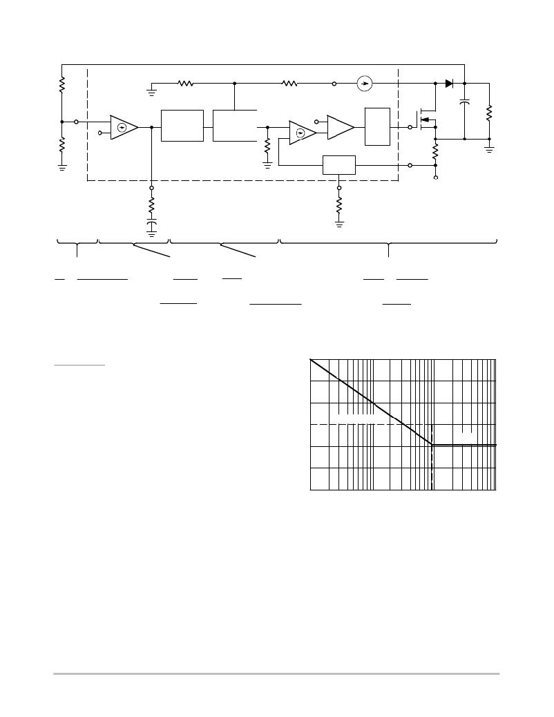
�Figure� 41.� Voltage� Loop� Model�
�Block� Diagram�
�The� block� diagram� for� the� voltage� loop� has� been� broken� down�
�into� four� sections.� These� are� the� voltage� divider,� voltage� error�
�20�
�amplifier,� reference� signal� and� modulator� and� output� stage.�
�The� modulator� and� output� stage� circuitry� is� greatly�
�simplified� based� on� the� assumption� that� that� poles� and� zeros�
�in� the� current� feedback� loop� are� considerably� greater� than�
�0�
�UNITY� GAIN�
�Av�
�the� bandwidth� of� the� overall� loop.� This� should� be� a� good�
�assumption,� because� a� bandwidth� in� the� kilohertz� is�
�necessary� for� a� good� current� waveform,� and� the� voltage� error�
�amplifier� needs� to� have� a� bandwidth� of� less� than� the� lowest�
�line� frequency� that� will� be� used.�
�There� are� two� poles� in� this� circuit.� The� output� filter� has� a�
�pole� that� varies� with� the� load.� The� pole� on� the� voltage� error�
�amplifier� will� be� determined� by� this� analysis.�
�Voltage� Divider�
�The� voltage� divider� is� a� simple� resistive� divider� that�
�reduces� the� output� voltage� to� the� 4.0� volt� level� required� by�
�the� internal� reference� on� the� voltage� error� amplifier.�
�Voltage� Error� Amplifier�
�The� voltage� error� amplifier� is� constrained� by� the� three�
�equations.� When� this� amplifier� is� compensated� with� a�
�pole--zero� pair,� there� will� be� a� unity� gain� pole� which� will� be�
�cancelled� by� the� zero� at� frequency� f� Z� .� The� corresponding�
�bode� plot� would� be:�
�--20�
�FREQUENCY�
�Figure� 42.� Pole--Zero� Bode� Plot�
�Reference� Signal�
�The� output� of� the� error� amplifier� is� modified� by� the� ORing�
�network,� which� has� a� negative� gain,� and� is� then� used� as� an�
�input� to� the� reference� multiplier.� The� gain� of� this� block� is�
�dependent� on� the� AC� input� voltage,� because� of� the� multiplier�
�which� requires� two� inputs� for� one� output.�
�Modulator� and� Output� Stage�
�The� AC� error� amplifier� receives� an� input� from� the�
�reference� multiplier� and� forces� the� current� to� follow� the�
�shape� and� amplitude� of� the� reference� signal.� The� current�
�shaping� circuit� is� an� internal� loop� within� this� section� due� to�
�the� current� sense� amplifier.� Based� on� the� assumptions� listed�
�http://onsemi.com�
�27�
�相关PDF资料 |
PDF描述 |
|---|---|
| NCP1652L48VGEVB | BOARD EVAL 100W 48V NCP1652 PFC |
| NCP1653EVB | BOARD EVAL FOR NCP1653 |
| NCP2993FCT2GEVB | BOARD EVAL NCP2993 AUDIO PWR AMP |
| NCP345SNT1G | IC DETECTOR OVER VOLTAGE 5TSOP |
| NCP346SN2T1G | IC DETECTOR OVER VOLTAGE 5TSOP |
相关代理商/技术参数 |
参数描述 |
|---|---|
| NCP1651DR2 | 功能描述:功率因数校正 IC Single Stage PFC RoHS:否 制造商:Fairchild Semiconductor 开关频率:300 KHz 最大功率耗散: 最大工作温度:+ 125 C 安装风格:SMD/SMT 封装 / 箱体:SOIC-8 封装:Reel |
| NCP1651DR2G | 功能描述:功率因数校正 IC Single Stage PFC RoHS:否 制造商:Fairchild Semiconductor 开关频率:300 KHz 最大功率耗散: 最大工作温度:+ 125 C 安装风格:SMD/SMT 封装 / 箱体:SOIC-8 封装:Reel |
| NCP1652ADR2G | 功能描述:功率因数校正 IC ANA PFC CONTROLLER RoHS:否 制造商:Fairchild Semiconductor 开关频率:300 KHz 最大功率耗散: 最大工作温度:+ 125 C 安装风格:SMD/SMT 封装 / 箱体:SOIC-8 封装:Reel |
| NCP1652DR2G | 功能描述:功率因数校正 IC ANA PFC CONTROLLER RoHS:否 制造商:Fairchild Semiconductor 开关频率:300 KHz 最大功率耗散: 最大工作温度:+ 125 C 安装风格:SMD/SMT 封装 / 箱体:SOIC-8 封装:Reel |
| NCP1652DWR2G | 功能描述:功率因数校正 IC ANA PFC CONTROLLER RoHS:否 制造商:Fairchild Semiconductor 开关频率:300 KHz 最大功率耗散: 最大工作温度:+ 125 C 安装风格:SMD/SMT 封装 / 箱体:SOIC-8 封装:Reel |
发布紧急采购,3分钟左右您将得到回复。