- 您现在的位置:买卖IC网 > PDF目录20432 > NCP3121QPBCKGEVB (ON Semiconductor)EVAL BOARD FOR NCP3121QPBCKG PDF资料下载
参数资料
| 型号: | NCP3121QPBCKGEVB |
| 厂商: | ON Semiconductor |
| 文件页数: | 1/41页 |
| 文件大小: | 0K |
| 描述: | EVAL BOARD FOR NCP3121QPBCKG |
| 设计资源: | NCP3121 EVB BOM NCP3121QPBCKGEVB Gerber Files NCP3121QPBCKGEVB Schematic |
| 标准包装: | 1 |
| 主要目的: | DC/DC,步降 |
| 输出及类型: | 2,非隔离 |
| 输出电压: | 3.3V,5V |
| 电流 - 输出: | 3A,3A |
| 输入电压: | 12V |
| 稳压器拓扑结构: | 降压 |
| 板类型: | 完全填充 |
| 已供物品: | 板 |
| 已用 IC / 零件: | NCP3121 |
| 其它名称: | NCP3121QPBCKGEVBOS |
当前第1页第2页第3页第4页第5页第6页第7页第8页第9页第10页第11页第12页第13页第14页第15页第16页第17页第18页第19页第20页第21页第22页第23页第24页第25页第26页第27页第28页第29页第30页第31页第32页第33页第34页第35页第36页第37页第38页第39页第40页第41页
�� �
�
�NCP3121�
�Dual� 3.0� A,� Step-Down�
�DC/DC� Switching� Regulator�
�The� NCP3121� is� a� dual� buck� converter� designed� for� low� voltage�
�applications� requiring� high� efficiency.� This� device� is� capable� of�
�G�
�producing� an� output� voltage� as� low� as� 0.8� V.� The� NCP3121� provides�
�dual� 3.0� A� switching� regulators� with� an� adjustable� 200� kHz� ?� 750� kHz�
�switching� frequency.� The� switching� frequency� is� set� by� an� external�
�resistor.� The� NCP3121� also� incorporates� an� auto� ?� tracking� and�
�sequencing� feature.� Protection� features� include� cycle� ?� by� ?� cycle�
�current� limit� and� undervoltage� lockout� (UVLO).� The� NCP3121� comes�
�in� a� 32� ?� pin� QFN� package.�
�Features�
�?� Input� Voltage� Range� from� 4.5� V� to� 13.2� V�
�?� 12� V� in� to� 5.0� V� out� =� 85%� Efficiency� Min� @� 3.0� A�
�?� 200� ?� 750� kHz� Operation�
�?� Stable� with� Low� ESR� Ceramic� Output� Capacitor�
�?� 0.8� ±� 1.5%� FB� Reference� Voltage�
�?� External� Soft� ?� Start�
�?� Out� of� Phase� Operation� of� OUT1� &� OUT2�
�?� Auto� ?� Tracking� and� Sequencing�
�?� Enable/Disable� Capability�
�?� Hiccup� Overload� Protection�
�?� Low� Shutdown� Power� (I� q� <� 100� m� A)�
�http://onsemi.com�
�MARKING� DIAGRAM�
�1�
�NCP3121�
�1� 32� AWLYYWW� G�
�QFN32�
�CASE� 488AM�
�NCP3121� =� Specific� Device� Code�
�A� =� Assembly� Location�
�WL� =� Wafer� Lot�
�YY� =� Year�
�WW� =� Work� Week�
�G� =� Pb� ?� Free� Package�
�(Note:� Microdot� may� be� in� either� location)�
�ORDERING� INFORMATION�
�See� detailed� ordering� and� shipping� information� in� the� package�
�dimensions� section� on� page� 40� of� this� data� sheet.�
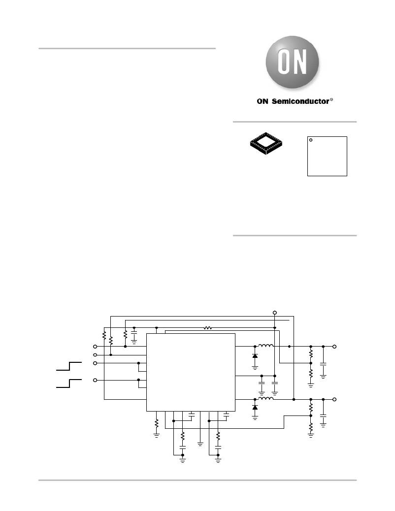
�Typical� Applications�
�?� Set� ?� Top� Boxes,� Portable� Applications,� Networking� and�
�Telecommunications�
�?� DSP/� m� P/FPGA� Core�
�VIN�
�RVIN�
�Disable�
�Disable�
�R_TRACK�
�PG1�
�PG2�
�Enable�
�EN1�
�Enable�
�EN2�
�R14�
�R24�
�C3�
�GND�
�PG1�
�PG2�
�EN1�
�SEQ1�
�EN2�
�SEQ2�
�NCP3121�
�SW1�
�VIN�
�C1�
�L11�
�D11�
�GND�
�C2�
�R11�
�R12�
�GND�
�OUT1�
�C11�
�GND�
�TRACK1,2�
�SW2�
�GND�
�GND�
�OUT2�
�L21�
�D21�
�R21�
�C21�
�RT�
�C22�
�C12�
�GND�
�R22�
�GND�
�R23�
�R13�
�GND�
�GND�
�C23�
�GND�
�C13�
�GND� GND�
�Figure� 1.� Typical� Application� Circuit�
�?� Semiconductor� Components� Industries,� LLC,� 2010�
�October,� 2010� ?� Rev.� 2�
�1�
�Publication� Order� Number:�
�NCP3121/D�
�相关PDF资料 |
PDF描述 |
|---|---|
| AT45DB321C-RU | IC FLASH 32MBIT 40MHZ 28SOIC |
| MIC4429BM | IC DRIVER MOSFET 6A LS 8-SOIC |
| SB550-E3/51 | DIODE SCHOTTKY 5A 50V DO-201AD |
| NCP3120QPBCKGEVB | EVAL BOARD FOR NCP3120QPBCKG |
| VF30100S-E3/45 | DIODE SCHOTTKY 30A 100V ITO220AB |
相关代理商/技术参数 |
参数描述 |
|---|---|
| NCP3122MNTXG | 功能描述:直流/直流开关调节器 Dual 2.0 Switching Regulator RoHS:否 制造商:International Rectifier 最大输入电压:21 V 开关频率:1.5 MHz 输出电压:0.5 V to 0.86 V 输出电流:4 A 输出端数量: 最大工作温度: 安装风格:SMD/SMT 封装 / 箱体:PQFN 4 x 5 |
| NCP3122QPBCKGEVB | 功能描述:电源管理IC开发工具 NCP3122 2A HF BUCK DB RoHS:否 制造商:Maxim Integrated 产品:Evaluation Kits 类型:Battery Management 工具用于评估:MAX17710GB 输入电压: 输出电压:1.8 V |
| NCP3123MNTXG | 功能描述:直流/直流开关调节器 Dual 3.0 A Switching Regulator RoHS:否 制造商:International Rectifier 最大输入电压:21 V 开关频率:1.5 MHz 输出电压:0.5 V to 0.86 V 输出电流:4 A 输出端数量: 最大工作温度: 安装风格:SMD/SMT 封装 / 箱体:PQFN 4 x 5 |
| NCP3123MNTXG-CUT TAPE | 制造商:ON 功能描述:NCP3123 Series 13.2 V Dual 3 A Step-Down DC/DC Switching Regulator - QFN-32 |
| NCP3123QPBCKGEVB | 功能描述:电源管理IC开发工具 NCP3123 3A HF BUCK DB RoHS:否 制造商:Maxim Integrated 产品:Evaluation Kits 类型:Battery Management 工具用于评估:MAX17710GB 输入电压: 输出电压:1.8 V |
发布紧急采购,3分钟左右您将得到回复。