- 您现在的位置:买卖IC网 > PDF目录20432 > NCP3121QPBCKGEVB (ON Semiconductor)EVAL BOARD FOR NCP3121QPBCKG PDF资料下载
参数资料
| 型号: | NCP3121QPBCKGEVB |
| 厂商: | ON Semiconductor |
| 文件页数: | 18/41页 |
| 文件大小: | 0K |
| 描述: | EVAL BOARD FOR NCP3121QPBCKG |
| 设计资源: | NCP3121 EVB BOM NCP3121QPBCKGEVB Gerber Files NCP3121QPBCKGEVB Schematic |
| 标准包装: | 1 |
| 主要目的: | DC/DC,步降 |
| 输出及类型: | 2,非隔离 |
| 输出电压: | 3.3V,5V |
| 电流 - 输出: | 3A,3A |
| 输入电压: | 12V |
| 稳压器拓扑结构: | 降压 |
| 板类型: | 完全填充 |
| 已供物品: | 板 |
| 已用 IC / 零件: | NCP3121 |
| 其它名称: | NCP3121QPBCKGEVBOS |
第1页第2页第3页第4页第5页第6页第7页第8页第9页第10页第11页第12页第13页第14页第15页第16页第17页当前第18页第19页第20页第21页第22页第23页第24页第25页第26页第27页第28页第29页第30页第31页第32页第33页第34页第35页第36页第37页第38页第39页第40页第41页
�� �
�
�NCP3121�
�Output� Voltage� Programming�
�The� controller� will� maintain� 0.8� V� at� the� feedback� pin.�
�Thus,� if� a� resistor� divider� circuit� is� placed� across� the�
�Table� 4.� Output� Voltage� Setting�
�feedback� pin� to� V� OUT� ,� the� controller� will� regulate� the� output�
�voltage� in� proportion� to� the� resistor� divider� network� in� order�
�to� maintain� 0.8� V� at� the� FB� pin.�
�V� OUT� [V]�
�R� 1� [k� W� ]�
�R� 2� [k� W� ]�
�8�
�180�
�20�
�7.5�
�360�
�43�
�6�
�130�
�20�
�5�
�68�
�13�
�4�
�300�
�75�
�3.3�
�47�
�15�
�2.5�
�51�
�24�
�1.8�
�20�
�16�
�1.2�
�10�
�20�
�V� OUT�
�R1�
�V� FB�
�R2�
�Figure� 36.� Feedback� divider�
�The� relationship� between� the� resistor� divider� network� and�
�the� output� voltage� is� shown� in� the� following� equation:�
�frequency� operation� because� a� higher� frequency� results� in�
�lower� efficiency� due� to� MOSFET� gate� charge� losses.�
�Additionally,� the� use� of� smaller� inductors� at� higher�
�frequencies� results� in� higher� ripple� current,� higher� output�
�voltage� ripple,� and� lower� efficiency� at� light� load� currents.�
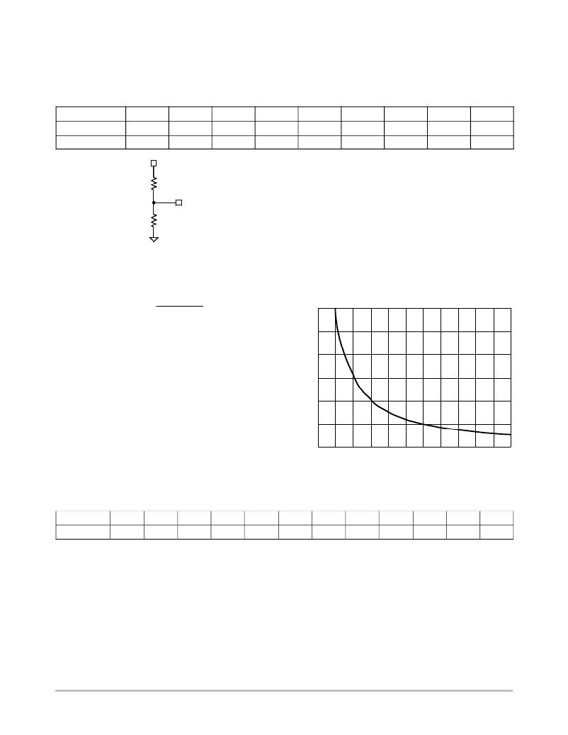
�The� value� of� the� oscillator� resistor� is� designed� to� be� linearly�
�related� to� the� switching� period.� There� are� two� ways� to�
�determine� the� RT� resistor� value:� by� using� the� standard� curve�
�shown� in� Figure� 37� or� by� using� Table� 5.� The� frequency� on�
�the� RT� pin� will� set� the� master� oscillator.� The� actual� operating�
�frequency� on� each� channel� will� be� one� ?� half� the� master�
�oscillator.�
�R� 2� +� R� 1�
�V� REF�
�V� OUT� *� V� REF�
�600�
�where:�
�V� REF� is� the� circuit’s� internal� voltage� reference,� which�
�equals� 0.8� V.�
�Resistor� R1� is� selected� based� on� a� design� trade� ?� off�
�between� efficiency� and� output� voltage� accuracy.� For� high�
�values� of� R1,� there� is� less� current� consumption� in� the�
�feedback� network.� However,� the� trade� ?� off� is� output� voltage�
�accuracy� due� to� the� bias� current� in� the� error� amplifier.� Once�
�R1� has� been� determined,� R2� can� be� calculated.�
�Selecting� the� Switching� Frequency�
�500�
�400�
�300�
�200�
�100�
�Selecting� the� switching� frequency� is� a� trade� ?� off� between�
�component� size� and� power� losses.� Operation� at� higher�
�switching� frequencies� allows� the� use� of� smaller� inductor� and�
�capacitor� values.� Nevertheless,� it� is� common� to� select� lower�
�Table� 5.� Switching� Frequency� Selection�
�0�
�200� 250� 300� 350� 400� 450� 500� 550� 600� 650� 700� 750�
�freq� [kHz]�
�Figure� 37.� Switching� Frequency� Selection�
�Freq.� [kHz]�
�RT� [k� W� ]�
�200�
�open�
�250�
�649�
�300�
�316�
�350�
�205�
�400�
�154�
�450�
�121�
�500�
�100�
�550�
�84.5�
�600�
�73.2�
�650�
�64.9�
�700�
�57.6�
�750�
�52.3�
�Sequencing� of� Output� Voltages�
�Some� microprocessors� and� DSP� chips� need� two� power�
�supplies� with� different� voltage� levels.� These� systems� often�
�require� voltage� sequencing� between� the� core� power� supply�
�and� the� I/O� power� supply.� Without� proper� sequencing,�
�latch� ?� up� failure� or� excessive� current� draw� may� occur� that�
�could� result� in� damage� to� the� processor’s� I/O� ports� or� the� I/O�
�ports� of� a� supporting� system� device� such� as� memory,� an�
�FPGA� or� a� data� converter.� To� ensure� that� the� I/O� loads� are�
�not� driven� until� the� core� voltage� is� properly� biased,� tracking�
�of� the� core� supply� and� the� I/O� supply� voltage� is� necessary.�
�Designing� a� system� without� proper� power� supply�
�sequencing� for� signal� processing� devices� like� DSPs,� FPGAs,�
�and� PLDs� may� create� risks� as� to� reliability� or� proper�
�functionality.� The� risk� comes� when� there� are� active� and�
�inactive� power� supply� rails� on� the� device� for� a� long� time.�
�During� this� time,� the� ESD� structures,� internal� circuits� and�
�components� are� stressed� from� interference� between�
�different� voltages� (from� the� two� separate� power� supply�
�rails).� When� these� conditions� persist� on� multi� ?� supply�
�devices� for� long� time� periods� (this� is� a� cumulative�
�phenomenon),� the� life� of� the� products� (DSP,� FPGA,� and�
�http://onsemi.com�
�18�
�相关PDF资料 |
PDF描述 |
|---|---|
| AT45DB321C-RU | IC FLASH 32MBIT 40MHZ 28SOIC |
| MIC4429BM | IC DRIVER MOSFET 6A LS 8-SOIC |
| SB550-E3/51 | DIODE SCHOTTKY 5A 50V DO-201AD |
| NCP3120QPBCKGEVB | EVAL BOARD FOR NCP3120QPBCKG |
| VF30100S-E3/45 | DIODE SCHOTTKY 30A 100V ITO220AB |
相关代理商/技术参数 |
参数描述 |
|---|---|
| NCP3122MNTXG | 功能描述:直流/直流开关调节器 Dual 2.0 Switching Regulator RoHS:否 制造商:International Rectifier 最大输入电压:21 V 开关频率:1.5 MHz 输出电压:0.5 V to 0.86 V 输出电流:4 A 输出端数量: 最大工作温度: 安装风格:SMD/SMT 封装 / 箱体:PQFN 4 x 5 |
| NCP3122QPBCKGEVB | 功能描述:电源管理IC开发工具 NCP3122 2A HF BUCK DB RoHS:否 制造商:Maxim Integrated 产品:Evaluation Kits 类型:Battery Management 工具用于评估:MAX17710GB 输入电压: 输出电压:1.8 V |
| NCP3123MNTXG | 功能描述:直流/直流开关调节器 Dual 3.0 A Switching Regulator RoHS:否 制造商:International Rectifier 最大输入电压:21 V 开关频率:1.5 MHz 输出电压:0.5 V to 0.86 V 输出电流:4 A 输出端数量: 最大工作温度: 安装风格:SMD/SMT 封装 / 箱体:PQFN 4 x 5 |
| NCP3123MNTXG-CUT TAPE | 制造商:ON 功能描述:NCP3123 Series 13.2 V Dual 3 A Step-Down DC/DC Switching Regulator - QFN-32 |
| NCP3123QPBCKGEVB | 功能描述:电源管理IC开发工具 NCP3123 3A HF BUCK DB RoHS:否 制造商:Maxim Integrated 产品:Evaluation Kits 类型:Battery Management 工具用于评估:MAX17710GB 输入电压: 输出电压:1.8 V |
发布紧急采购,3分钟左右您将得到回复。