- 您现在的位置:买卖IC网 > PDF目录20432 > NCP3121QPBCKGEVB (ON Semiconductor)EVAL BOARD FOR NCP3121QPBCKG PDF资料下载
参数资料
| 型号: | NCP3121QPBCKGEVB |
| 厂商: | ON Semiconductor |
| 文件页数: | 36/41页 |
| 文件大小: | 0K |
| 描述: | EVAL BOARD FOR NCP3121QPBCKG |
| 设计资源: | NCP3121 EVB BOM NCP3121QPBCKGEVB Gerber Files NCP3121QPBCKGEVB Schematic |
| 标准包装: | 1 |
| 主要目的: | DC/DC,步降 |
| 输出及类型: | 2,非隔离 |
| 输出电压: | 3.3V,5V |
| 电流 - 输出: | 3A,3A |
| 输入电压: | 12V |
| 稳压器拓扑结构: | 降压 |
| 板类型: | 完全填充 |
| 已供物品: | 板 |
| 已用 IC / 零件: | NCP3121 |
| 其它名称: | NCP3121QPBCKGEVBOS |
第1页第2页第3页第4页第5页第6页第7页第8页第9页第10页第11页第12页第13页第14页第15页第16页第17页第18页第19页第20页第21页第22页第23页第24页第25页第26页第27页第28页第29页第30页第31页第32页第33页第34页第35页当前第36页第37页第38页第39页第40页第41页
�� �
�
�NCP3121�
�Loop� Compensation�
�A� COMP� pin� of� the� transconductance� error� amplifier� is�
�used� to� compensate� the� regulation� control� system.� Standard�
�COMP� pin� values� are� shown� in� the� BOM� at� the� end� of� the�
�datasheet.� (See� the� COMPCALC� program� to� determine�
�customer� preferred� values.)�
�To� design� the� compensation� components� for� conditions�
�not� described� in� Table� 6� and/or� for� tuning� the� compensation�
�for� specific� requirements,� the� COMPCALC� design� tool� is�
�available� from� ON� Semiconductor� at� no� charge.� Visit�
�http://www.onsemi.com/pub/Collateral/COMPCALC.ZIP�
�to� download� the� self� ?� extracting� program� for� NCP3121� loop�
�compensation� design� assistance.� There� is� an� Excel� design�
�tool� for� component� selection.� This� design� tool� is� available� at�
�http://www.onsemi.com/pub/Collateral/NCP312X%20�
�DWS.XLS� .�
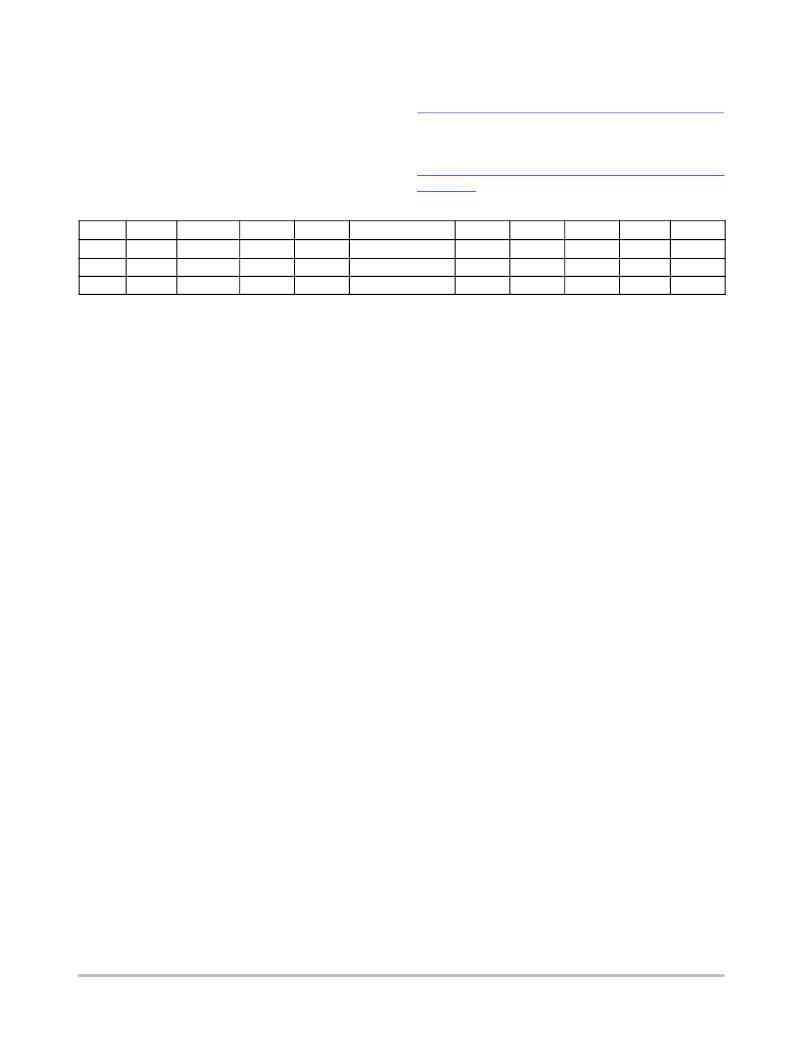
�Table� 6.� Compensation� Values� Example� for� Typical� Output� Voltages�
�Vin� [V]�
�12�
�12�
�5�
�Vout� [V]�
�3.3�
�5�
�1.8�
�Freq� [kHz]�
�200�
�200�
�200�
�Iout� [A]�
�3�
�3�
�3�
�L11� [� m� H]�
�15�
�22�
�10�
�C11� ?� ceramic� [� m� F]�
�22�
�22�
�22�
�C13� [nF]�
�22�
�18�
�27�
�R13� [k� W� ]�
�4.7�
�4.7�
�2.7�
�C14� [pF]�
�220�
�270�
�270�
�R14� [� W� ]�
�100�
�100�
�100�
�C15� [nF]�
�none�
�none�
�none�
�Thermal� Considerations�
�The� NCP3121� has� thermal� shutdown� protection� to�
�safeguard� the� device� from� overheating� when� the� die�
�temperature� exceeds� 160� _� C.� For� the� best� thermal�
�performance,� wide� copper� traces� and� a� generous� amount� of�
�PCB� printed� circuit� board� copper� should� be� used� in� the� board�
�layout.� One� exception� to� this� is� at� the� SW� switching� node,�
�which� should� not� have� a� large� area� in� order� to� minimize� the�
�EMI� radiation� and� other� parasitic� effects.� Large� areas� of�
�copper� provide� the� best� transfer� of� heat� from� the� IC� into� the�
�ambient� air.�
�PCB� Layout� Guidelines�
�As� in� any� switching� regulator,� the� layout� of� the� printed�
�circuit� board� is� very� important.� Rapidly� switching� currents�
�associated� with� wiring� inductance,� stray� capacitance� and�
�parasitic� inductance� of� the� printed� circuit� board� traces� can�
�generate� voltage� transients� that� can� generate�
�electromagnetic� interferences� (EMI)� and� affect� the� desired�
�operation.� To� minimize� inductance� and� ground� loops,� the�
�lengths� of� the� leads� indicated� by� heavy� lines� should� be� kept�
�as� short� as� possible.� For� best� results,� single� ?� point� grounding�
�or� ground� plane� construction� should� be� used.� On� the� other�
�hand,� the� PCB� area� connected� to� the� SW� pin� (drain� of� the�
�internal� switch)� of� the� circuit� should� be� kept� to� a� minimum�
�in� order� to� minimize� coupling� to� sensitive� circuitry.� Another�
�sensitive� part� of� the� circuit� is� the� feedback.� It� is� important� to�
�keep� the� sensitive� feedback� wiring� short.� To� ensure� this,�
�physically� locate� the� programming� resistors� near� the�
�regulator.�
�There� should� be� a� ground� area� on� the� top� layer� directly�
�under� the� IC� with� an� exposed� area� for� connecting� the� IC�
�exposed� pad.� Any� internal� ground� planes� should� be�
�connected� by� vias� to� this� ground� area.� Additional� vias� must�
�be� used� at� the� ground� side� of� the� input� and� output� capacitors.�
�The� GND� pin� also� should� be� tied� to� the� PCB� ground� in� the�
�area� under� the� IC.�
�When� laying� out� the� buck� regulator� on� a� printed� circuit�
�board,� the� following� checklist� should� be� used� to� ensure�
�proper� operation� of� the� circuit:�
�1.� Rapid� changes� in� voltage� across� parasitic�
�capacitors� and� abrupt� changes� in� current� in�
�parasitic� inductors� are� major� concerns� for� a� good�
�layout.�
�2.� Keep� high� currents� out� of� sensitive� ground�
�connections.�
�3.� Avoid� ground� loops,� as� they� pick� up� noise.� Use�
�star� or� single� ?� point� grounding.�
�4.� For� high� power� buck� regulators� on� double� ?� sided�
�PCBs,� a� single� ground� plane� (usually� the� bottom)�
�is� recommended.�
�5.� Even� though� double� ?� sided� PCBs� are� usually�
�sufficient� for� a� good� layout,� four� layer� PCBs�
�represent� the� optimum� approach� to� reducing�
�susceptibility� to� noise.� Use� the� two� internal� layers�
�as� the� power� and� GND� planes,� the� top� layer� for�
�power� connections� and� component� vias,� and� the�
�bottom� layer� for� noise� sensitive� traces.�
�6.� Keep� the� inductor� switching� node� small� by� placing�
�the� output� inductor� as� close� as� possible� to� the� chip.�
�7.� Use� fewer,� but� larger,� output� capacitors;� keep� the�
�capacitors� clustered;� and� use� multiple� layer� traces�
�with� heavy� copper� to� keep� the� parasitic� resistance�
�low.�
�8.� Place� the� output� capacitors� as� close� to� the� output�
�coil� as� possible.�
�9.� Place� the� COMP� capacitor� as� close� as� possible� to�
�the� COMP� pin.�
�10.� Place� the� V� IN� bypass� capacitors� as� close� as�
�possible� to� the� IC.�
�11.� Place� the� RT� resistor� as� close� as� possible� to� the� RT�
�pin.�
�12.� The� exposed� pad� must� be� connected� to� a� ground�
�plane� with� a� large� copper� surface� area� to� dissipate�
�heat.�
�http://onsemi.com�
�36�
�相关PDF资料 |
PDF描述 |
|---|---|
| AT45DB321C-RU | IC FLASH 32MBIT 40MHZ 28SOIC |
| MIC4429BM | IC DRIVER MOSFET 6A LS 8-SOIC |
| SB550-E3/51 | DIODE SCHOTTKY 5A 50V DO-201AD |
| NCP3120QPBCKGEVB | EVAL BOARD FOR NCP3120QPBCKG |
| VF30100S-E3/45 | DIODE SCHOTTKY 30A 100V ITO220AB |
相关代理商/技术参数 |
参数描述 |
|---|---|
| NCP3122MNTXG | 功能描述:直流/直流开关调节器 Dual 2.0 Switching Regulator RoHS:否 制造商:International Rectifier 最大输入电压:21 V 开关频率:1.5 MHz 输出电压:0.5 V to 0.86 V 输出电流:4 A 输出端数量: 最大工作温度: 安装风格:SMD/SMT 封装 / 箱体:PQFN 4 x 5 |
| NCP3122QPBCKGEVB | 功能描述:电源管理IC开发工具 NCP3122 2A HF BUCK DB RoHS:否 制造商:Maxim Integrated 产品:Evaluation Kits 类型:Battery Management 工具用于评估:MAX17710GB 输入电压: 输出电压:1.8 V |
| NCP3123MNTXG | 功能描述:直流/直流开关调节器 Dual 3.0 A Switching Regulator RoHS:否 制造商:International Rectifier 最大输入电压:21 V 开关频率:1.5 MHz 输出电压:0.5 V to 0.86 V 输出电流:4 A 输出端数量: 最大工作温度: 安装风格:SMD/SMT 封装 / 箱体:PQFN 4 x 5 |
| NCP3123MNTXG-CUT TAPE | 制造商:ON 功能描述:NCP3123 Series 13.2 V Dual 3 A Step-Down DC/DC Switching Regulator - QFN-32 |
| NCP3123QPBCKGEVB | 功能描述:电源管理IC开发工具 NCP3123 3A HF BUCK DB RoHS:否 制造商:Maxim Integrated 产品:Evaluation Kits 类型:Battery Management 工具用于评估:MAX17710GB 输入电压: 输出电压:1.8 V |
发布紧急采购,3分钟左右您将得到回复。