- 您现在的位置:买卖IC网 > PDF目录20432 > NCP3121QPBCKGEVB (ON Semiconductor)EVAL BOARD FOR NCP3121QPBCKG PDF资料下载
参数资料
| 型号: | NCP3121QPBCKGEVB |
| 厂商: | ON Semiconductor |
| 文件页数: | 21/41页 |
| 文件大小: | 0K |
| 描述: | EVAL BOARD FOR NCP3121QPBCKG |
| 设计资源: | NCP3121 EVB BOM NCP3121QPBCKGEVB Gerber Files NCP3121QPBCKGEVB Schematic |
| 标准包装: | 1 |
| 主要目的: | DC/DC,步降 |
| 输出及类型: | 2,非隔离 |
| 输出电压: | 3.3V,5V |
| 电流 - 输出: | 3A,3A |
| 输入电压: | 12V |
| 稳压器拓扑结构: | 降压 |
| 板类型: | 完全填充 |
| 已供物品: | 板 |
| 已用 IC / 零件: | NCP3121 |
| 其它名称: | NCP3121QPBCKGEVBOS |
第1页第2页第3页第4页第5页第6页第7页第8页第9页第10页第11页第12页第13页第14页第15页第16页第17页第18页第19页第20页当前第21页第22页第23页第24页第25页第26页第27页第28页第29页第30页第31页第32页第33页第34页第35页第36页第37页第38页第39页第40页第41页
�� �
�
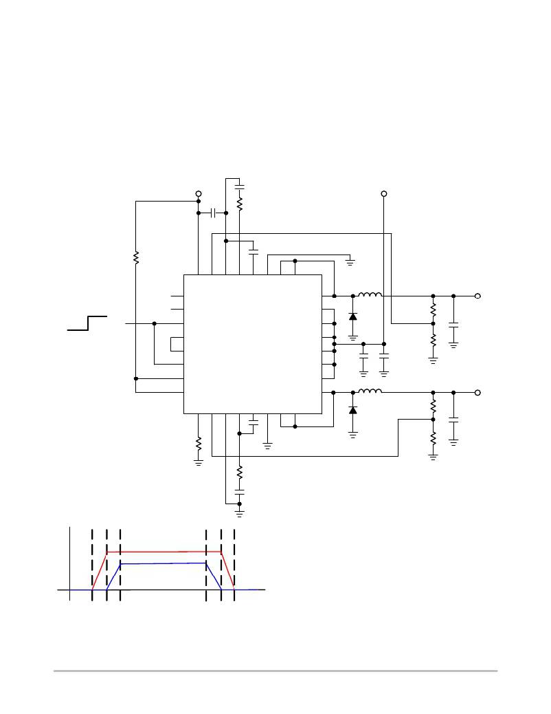
�NCP3121�
�Sequential� Sequencing� (First� ?� Up/Last� ?� Down�
�Sequence� Configuration)�
�In� sequential� sequencing� mode,� the� second� output� voltage�
�starts� ramping� when� the� first� output� voltage� is� already� settled�
�and� its� power� good� signal� is� set.� Figure� 44� shows� the�
�NCP3121’s� configuration� and� standard� waveforms.� The�
�rising� slope� of� both� voltages� can� be� selected� independently�
�by� the� soft� ?� start� capacitors’� values� (C12,� C22).� When� the�
�enable� pin� is� deactivated,� the� second� output� voltage�
�decreases� first,� followed� by� the� first� output� voltage.� The�
�control� logic� is� based� on� the� internal� power� good� signal;� no�
�delay� is� added.� The� signal� has� the� same� threshold� values� as�
�the� power� good� signal� shown� in� the� electrical� table.� The�
�sequential� sequencing� mode� is� also� called� first� ?� up/�
�last� ?� down� and� is� ideal� for� DSPs� with� separate� power�
�supplies� for� the� core� and� the� I/O� ports.�
�Note:� If� enable� control� is� not� required,� float� the�
�EN(first)/SEQ(last)� connection� rather� than� pulling� it� to� VIN�
�or� a� separate� supply� voltage.� For� Figure� 44� this� is�
�EN1/SEQ1.� For� Figure� 45,� this� is� EN1/SEQ4.� The�
�NCP3121� will� enable� itself� once� VIN� crosses� the� input�
�UVLO� threshold.�
�R_TRACK�
�AVIN�
�C3�
�C13�
�R13�
�C12�
�GND�
�VIN�
�OUT1�
�Disable�
�Enable�
�EN1�
�PG1�
�PG2�
�EN1�
�SW1�
�VIN�
�VIN�
�L11�
�D11�
�R11�
�C11�
�SEQ1�
�EN2�
�SEQ2�
�TRACK1�
�TRACK2�
�NCP3121�
�VIN�
�VIN�
�VIN�
�VIN�
�SW2�
�C1�
�GND�
�GND�
�L21�
�C2�
�GND�
�R12�
�GND�
�GND�
�OUT2�
�D21�
�R21�
�C21�
�R_T�
�C22�
�GND�
�GND�
�R22�
�GND�
�C12� C22�
�GND�
�C22� C12�
�R23�
�C23�
�GND�
�GND�
�VOUT1�
�VOUT2�
�Figure� 44.� Sequential� Configuration�
�http://onsemi.com�
�21�
�相关PDF资料 |
PDF描述 |
|---|---|
| AT45DB321C-RU | IC FLASH 32MBIT 40MHZ 28SOIC |
| MIC4429BM | IC DRIVER MOSFET 6A LS 8-SOIC |
| SB550-E3/51 | DIODE SCHOTTKY 5A 50V DO-201AD |
| NCP3120QPBCKGEVB | EVAL BOARD FOR NCP3120QPBCKG |
| VF30100S-E3/45 | DIODE SCHOTTKY 30A 100V ITO220AB |
相关代理商/技术参数 |
参数描述 |
|---|---|
| NCP3122MNTXG | 功能描述:直流/直流开关调节器 Dual 2.0 Switching Regulator RoHS:否 制造商:International Rectifier 最大输入电压:21 V 开关频率:1.5 MHz 输出电压:0.5 V to 0.86 V 输出电流:4 A 输出端数量: 最大工作温度: 安装风格:SMD/SMT 封装 / 箱体:PQFN 4 x 5 |
| NCP3122QPBCKGEVB | 功能描述:电源管理IC开发工具 NCP3122 2A HF BUCK DB RoHS:否 制造商:Maxim Integrated 产品:Evaluation Kits 类型:Battery Management 工具用于评估:MAX17710GB 输入电压: 输出电压:1.8 V |
| NCP3123MNTXG | 功能描述:直流/直流开关调节器 Dual 3.0 A Switching Regulator RoHS:否 制造商:International Rectifier 最大输入电压:21 V 开关频率:1.5 MHz 输出电压:0.5 V to 0.86 V 输出电流:4 A 输出端数量: 最大工作温度: 安装风格:SMD/SMT 封装 / 箱体:PQFN 4 x 5 |
| NCP3123MNTXG-CUT TAPE | 制造商:ON 功能描述:NCP3123 Series 13.2 V Dual 3 A Step-Down DC/DC Switching Regulator - QFN-32 |
| NCP3123QPBCKGEVB | 功能描述:电源管理IC开发工具 NCP3123 3A HF BUCK DB RoHS:否 制造商:Maxim Integrated 产品:Evaluation Kits 类型:Battery Management 工具用于评估:MAX17710GB 输入电压: 输出电压:1.8 V |
发布紧急采购,3分钟左右您将得到回复。