参数资料
| 型号: | NCP5314MNR2 |
| 厂商: | ON Semiconductor |
| 文件页数: | 13/29页 |
| 文件大小: | 0K |
| 描述: | IC CTRLR BUCK CPU 2/3/4PH 32QFN |
| 产品变化通告: | Product Discontinuation 30/Jun/2004 |
| 标准包装: | 1 |
| 应用: | 控制器,CPU |
| 输入电压: | 9.5 V ~ 13.2 V |
| 输出数: | 4 |
| 工作温度: | 0°C ~ 70°C |
| 安装类型: | 表面贴装 |
| 封装/外壳: | 32-VFQFN 裸露焊盘 |
| 供应商设备封装: | 32-QFN(5x5) |
| 包装: | 剪切带 (CT) |
| 其它名称: | NCP5314MNR2OSCT |
第1页第2页第3页第4页第5页第6页第7页第8页第9页第10页第11页第12页当前第13页第14页第15页第16页第17页第18页第19页第20页第21页第22页第23页第24页第25页第26页第27页第28页第29页
�� �
�
�NCP5314�
�THEORY� OF� OPERATION�
�Overview�
�The� NCP5314� DC/DC� controller� from� ON� Semiconductor�
�was� developed� using� the� Enhanced� V� 2� topology.� Enhanced�
�V� 2� combines� the� original� V� 2� topology� with� peak�
�current?mode� control� for� fast� transient� response� and� current�
�sensing� capability.� The� addition� of� an� internal� PWM� ramp�
�and� implementation� of� fast?feedback� directly� from� Vcore�
�has� improved� transient� response� and� simplified� design.� This�
�controller� can� be� adjusted� to� operate� as� a� two?,� three?� or�
�four?phase� controller.� Differential� current� sensing� provides�
�improved� current� sharing� and� easier� layout.� The� NCP5314�
�includes� Power� Good� (PWRGD),� providing� a� highly�
�integrated� solution� to� simplify� design,� minimize� circuit�
�board� area,� and� reduce� overall� system� cost.�
�Two� advantages� of� a� multi?phase� converter� over� a�
�single?phase� converter� are� current� sharing� and� increased�
�effective� output� frequency.� Current� sharing� allows� the� designer�
�to� use� less� inductance� in� each� phase� than� would� be� required� in�
�a� single?phase� converter.� The� smaller� inductor� will� produce�
�larger� ripple� currents� but� the� total� per?phase� power� dissipation�
�is� reduced� because� the� RMS� current� is� lower.� Transient�
�response� is� improved� because� the� control� loop� will� measure�
�and� adjust� the� current� faster� with� a� smaller� output� inductor.�
�Increased� effective� output� frequency� is� desirable� because�
�the� off?time� and� the� ripple� voltage� of� the� multi?phase�
�converter� will� be� less� than� that� of� a� single?phase� converter.�
�x� =� 1,� 2,� 3� or� 4�
�Fixed� Frequency� Multi?Phase� Control�
�In� a� multi?phase� converter,� multiple� converters� are�
�connected� in� parallel� and� are� switched� on� at� different� times.�
�This� reduces� output� current� from� the� individual� converters�
�and� increases� the� ripple� frequency.� Because� several�
�converters� are� connected� in� parallel,� output� current� can� ramp�
�up� or� down� faster� than� a� single� converter� (with� the� same�
�value� output� inductor)� and� heat� is� spread� among� multiple�
�components.�
�The� NCP5314� controller� uses� four?phase,� fixed?frequency,�
�Enhanced� V� 2� architecture� to� measure� and� control� currents� in�
�individual� phases.� In� four� phase� mode,� each� phase� is�
�delayed� 90� °� from� the� previous� phase� (120� °� in� three?phase�
�mode).� Normally,� GATEx� transitions� to� a� high� voltage� at�
�the� beginning� of� each� oscillator� cycle.� Inductor� current�
�ramps� up� until� the� combination� of� the� amplified� current�
�sense� signal,� the� internal� ramp� and� the� output� voltage� ripple�
�trip� the� PWM� comparator� and� bring� GATEx� low.� Once�
�GATEx� goes� low,� it� will� remain� low� until� the� beginning� of�
�the� next� oscillator� cycle.� While� GATEx� is� high,� the�
�Enhanced� V� 2� loop� will� respond� to� line� and� load� variations.�
�On� the� other� hand,� once� GATEx� is� low,� the� loop� cannot�
�respond� until� the� beginning� of� the� next� PWM� cycle.�
�Therefore,� constant� frequency� Enhanced� V� 2� will� typically�
�respond� to� disturbances� within� the� off?time� of� the�
�converter.�
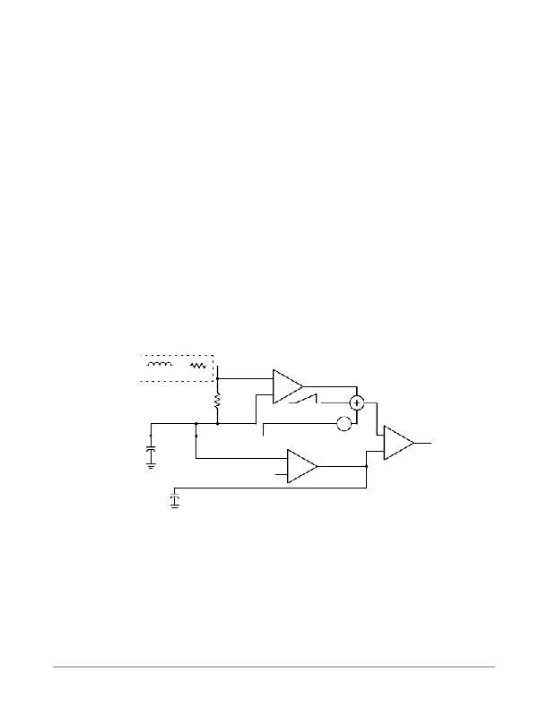
�SWNODE�
�Lx�
�RLx�
�CSxP�
�+�
�CSA�
�COx�
�RSx�
�CSxN�
�?�
�V� FFB�
�Internal� Ramp�
�V� OUT�
�(V� CORE� )�
�+�
�V� FB�
�“Fast?Feedback”�
�Connection�
�?�
�Channel�
�Startup�
�Offset�
�+�
�?�
�PWM�
�To� F/F�
�Reset�
�COMP�
�DAC�
�Out�
�E.A.�
�+�
�COMP�
�+�
�Figure� 17.� Enhanced� V� 2� Control� Employing� Resistive� Current� Sensing� and� Internal� Ramp�
�The� Enhanced� V� 2� architecture� measures� and� adjusts� the�
�output� current� in� each� phase.� An� additional� differential� input�
�(CSxN� and� CSxP)� for� inductor� current� information� has� been�
�added� to� the� V� 2� loop� for� each� phase� as� shown� in� Figure� 17.�
�The� triangular� inductor� current� is� measured� differentially�
�across� RS,� amplified� by� CSA� and� summed� with� the� channel�
�startup� offset,� the� internal� ramp� and� the� output� voltage� at� the�
�non?inverting� input� of� the� PWM� comparator.� The� purpose�
�of� the� internal� ramp� is� to� compensate� for� propagation� delays�
�in� the� NCP5314.� This� provides� greater� design� flexibility� by�
�widths,� higher� frequency� operation� and� PWM� duty� cycles�
�above� 50%� without� external� slope� compensation.� As� the�
�sum� of� the� inductor� current� and� the� internal� ramp� increase,�
�the� voltage� on� the� positive� pin� of� the� PWM� comparator� rises�
�and� terminates� the� PWM� cycle.� If� the� inductor� starts� a� cycle�
�with� higher� current,� the� PWM� cycle� will� terminate� earlier�
�providing� negative� feedback.� The� NCP5314� provides� a�
�differential� current� sense� input� (CSxN� and� CSxP)� for� each�
�phase.� Current� sharing� is� accomplished� by� referencing� all�
�phases� to� the� same� COMP� pin,� so� that� a� phase� with� a� larger�
�allowing� smaller� external� ramps,� lower� minimum� pulse�
�http://onsemi.com�
�13�
�相关PDF资料 |
PDF描述 |
|---|---|
| X4323S8-4.5A | IC SUPERVISOR CPU 32K EE 8-SOIC |
| EMC31DREF-S13 | CONN EDGECARD 62POS .100 EXTEND |
| RBM43DCSI | CONN EDGECARD 86POS DIP .156 SLD |
| P1812R-224K | INDUCTOR POWER 220UH SMD |
| X4323S8-2.7A | IC SUPERVISOR CPU 32K EE 8-SOIC |
相关代理商/技术参数 |
参数描述 |
|---|---|
| NCP5316 | 制造商:ONSEMI 制造商全称:ON Semiconductor 功能描述:Four/Five/Six−Phase Buck CPU Controller |
| NCP5316/D | 制造商:ONSEMI 制造商全称:ON Semiconductor 功能描述:Four/Five/Six-Phase Buck CPU Controller |
| NCP5316_06 | 制造商:ONSEMI 制造商全称:ON Semiconductor 功能描述:Four/Five/Six−Phase Buck CPU Controller |
| NCP5316FTR2 | 功能描述:IC CTRLR BUCK CPU 4/5/6PH 48LQFP RoHS:否 类别:集成电路 (IC) >> PMIC - 稳压器 - 专用型 系列:- 产品培训模块:Lead (SnPb) Finish for COTS Obsolescence Mitigation Program 标准包装:2,000 系列:- 应用:电源,ICERA E400,E450 输入电压:4.1 V ~ 5.5 V 输出数:10 输出电压:可编程 工作温度:-40°C ~ 85°C 安装类型:表面贴装 封装/外壳:42-WFBGA,WLCSP 供应商设备封装:42-WLP 包装:带卷 (TR) |
| NCP5316MNR2 | 功能描述:IC CTRLR BUCK CPU 4/5/6PH 48QFN RoHS:否 类别:集成电路 (IC) >> PMIC - 稳压器 - 专用型 系列:- 产品培训模块:Lead (SnPb) Finish for COTS Obsolescence Mitigation Program 标准包装:2,000 系列:- 应用:电源,ICERA E400,E450 输入电压:4.1 V ~ 5.5 V 输出数:10 输出电压:可编程 工作温度:-40°C ~ 85°C 安装类型:表面贴装 封装/外壳:42-WFBGA,WLCSP 供应商设备封装:42-WLP 包装:带卷 (TR) |
发布紧急采购,3分钟左右您将得到回复。