参数资料
| 型号: | NCP5314MNR2 |
| 厂商: | ON Semiconductor |
| 文件页数: | 17/29页 |
| 文件大小: | 0K |
| 描述: | IC CTRLR BUCK CPU 2/3/4PH 32QFN |
| 产品变化通告: | Product Discontinuation 30/Jun/2004 |
| 标准包装: | 1 |
| 应用: | 控制器,CPU |
| 输入电压: | 9.5 V ~ 13.2 V |
| 输出数: | 4 |
| 工作温度: | 0°C ~ 70°C |
| 安装类型: | 表面贴装 |
| 封装/外壳: | 32-VFQFN 裸露焊盘 |
| 供应商设备封装: | 32-QFN(5x5) |
| 包装: | 剪切带 (CT) |
| 其它名称: | NCP5314MNR2OSCT |
第1页第2页第3页第4页第5页第6页第7页第8页第9页第10页第11页第12页第13页第14页第15页第16页当前第17页第18页第19页第20页第21页第22页第23页第24页第25页第26页第27页第28页第29页
�� �
�
�NCP5314�
�VLOWER� +� VID� @� 1�
�Since� the� internally?set� thresholds� for� PWRLS� are� VID/2�
�for� the� lower� threshold� and� VID� +� 80� mV� for� the� upper�
�threshold,� a� simple� equation� can� be� provided� to� assist� the�
�designer� in� selecting� a� resistor� divider� to� provide� the� desired�
�PWRGD� performance.�
�V� R� )� R2�
�2� R1�
�VUPPER� +� VVID� )� 80� mV�
�The� logic� circuitry� inside� the� chip� sets� PWRGD� low� only�
�after� a� delay� period� has� been� passed.� A� “power� bad”� event�
�does� not� cause� PWRGD� to� go� low� unless� it� is� sustained�
�through� the� delay� time� of� 250� μ� s.� If� the� anomaly� disappears�
�before� the� end� of� the� delay,� the� PWRGD� output� will� never�
�be� set� low.�
�In� order� to� use� the� PWRGD� pin� as� specified,� the� user� is�
�advised� to� connect� external� resistors� as� necessary� to� limit� the�
�current� into� this� pin� to� 4� mA� or� less.�
�low� until� the� COMP� voltage� reaches� 0.6� V.� Once� this�
�threshold� is� reached,� the� GATE� outputs� are� released� to�
�operate� normally.�
�Current� Limit�
�Two� levels� of� over?current� protection� are� provided.� First,�
�if� the� voltage� between� the� Current� Sense� pins� (CSxN� and�
�CSxP)� exceeds� the� fixed� threshold� (Single� Pulse� Current�
�Limit),� the� PWM� comparator� is� turned� off.� This� provides�
�fast� peak� current� protection� for� individual� phases.� Second,�
�the� individual� phase� currents� are� summed� and� externally�
�low?pass� filtered� to� compare� an� averaged� current� signal� to�
�a� user� adjustable� voltage� on� the� I� LIM� pin.� If� the� I� LIM� voltage�
�is� exceeded,� the� fault� latch� trips� and� the� converter� is� latched�
�off.� V� CC� must� be� recycled� to� reset� the� latch.�
�Fault� Protection� Logic�
�The� NCP5314� includes� fault� protection� circuitry� to�
�prevent� harmful� modes� of� operation� from� occurring.� The�
�fault� logic� is� described� in� Table� 1.�
�PWRGD�
�HIGH�
�PWRGD�
�lo-�
�w�
�PWRGD�
�high�
�PWRGD�
�low�
�Gate� Outputs�
�The� NCP5314� is� designed� to� operate� with� external� gate�
�drivers.� Accordingly,� the� gate� outputs� are� capable� of� driving�
�a� 100� pF� load� with� typical� rise� and� fall� times� of� 5� ns.�
�LOW�
�Digital� to� Analog� Converter� (DAC)�
�?2.6%� +2.6�
�%�
�V� LOWER�
�?5.0%� +5.0�
�%�
�VID� +� 80� mV�
�V� OUT�
�The� output� voltage� of� the� NCP5314� is� set� by� means� of� a�
�6?bit,� 0.5%� DAC.� The� VID� pins� must� be� pulled� high�
�externally.� A� 1.5� k� Ω� pullup� to� a� maximum� of� 3.3� V� is�
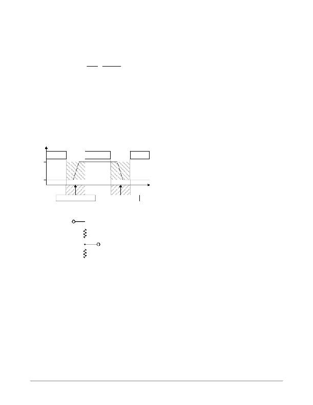
�Figure� 22.� PWRGD� Assertion� Window�
�V� OUT�
�R1�
�PWRLS�
�R2�
�recommended� to� meet� Intel� specifications.� To� ensure� valid�
�logic� signals,� the� designer� should� ensure� at� least� 800� mV� will�
�be� present� at� the� IC� for� a� logic� high.�
�The� output� of� the� DAC� is� described� in� the� Electrical�
�Characteristics� section� of� the� data� sheet.� These� outputs� are�
�consistent� with� VR10.x� and� processor� specifications.� The�
�DAC� output� is� 20� mV� below� the� VID� code� specification.�
�The� latest� VRM� and� processor� specifications� require� a�
�power� supply� to� turn� its� output� off� in� the� event� of� a� 11111X�
�VID� code.� When� the� DAC� sees� such� a� code,� the� GATE� pins�
�stop� switching� and� go� low.� This� condition� is� described� in�
�Table� 1.�
�Figure� 23.� Adjusting� the� PWRGD� Threshold�
�Adjusting� the� Number� of� Phases�
�Undervoltage� Lockout�
�The� NCP5314� includes� an� undervoltage� lockout� circuit.�
�This� circuit� keeps� the� IC’s� output� drivers� low� until� V� CC�
�applied� to� the� IC� reaches� 9� V.� The� GATE� outputs� are� disabled�
�when� V� CC� drops� below� 8� V.�
�Soft?Start�
�At� initial� power?up,� both� SS� and� COMP� voltages� are� zero.�
�The� total� SS� capacitance� will� begin� to� charge� with� a� current�
�of� 40� μ� A.� The� error� amplifier� directly� charges� the� COMP�
�capacitance.� An� internal� clamp� ensures� that� the� COMP� pin�
�voltage� will� always� be� less� than� the� voltage� at� the� SS� pin,�
�The� NCP5314� was� designed� with� a� selectable?phase�
�architecture.� Designers� may� choose� any� number� of� phases�
�up� to� four.� The� phase� delay� is� automatically� adjusted� to�
�match� the� number� of� phases� that� will� be� used.� This� feature�
�allows� the� designer� to� select� the� number� of� phases� required�
�for� a� particular� application.�
�Four?phase� operation� is� standard.� All� phases� switch� with�
�a� 90� degree� delay� between� pulses.� No� special� connections�
�are� required.�
�Three?phase� operation� is� achieved� by� disabling� phase� 4.�
�Tie� together� CS4N� and� CS4P,� and� then� pull� both� pins� to� V� CC� .�
�The� remaining� phases� will� continue� to� switch,� but� now� there�
�ensuring� proper� startup� behavior.� All� GATE� outputs� are� held�
�http://onsemi.com�
�17�
�相关PDF资料 |
PDF描述 |
|---|---|
| X4323S8-4.5A | IC SUPERVISOR CPU 32K EE 8-SOIC |
| EMC31DREF-S13 | CONN EDGECARD 62POS .100 EXTEND |
| RBM43DCSI | CONN EDGECARD 86POS DIP .156 SLD |
| P1812R-224K | INDUCTOR POWER 220UH SMD |
| X4323S8-2.7A | IC SUPERVISOR CPU 32K EE 8-SOIC |
相关代理商/技术参数 |
参数描述 |
|---|---|
| NCP5316 | 制造商:ONSEMI 制造商全称:ON Semiconductor 功能描述:Four/Five/Six−Phase Buck CPU Controller |
| NCP5316/D | 制造商:ONSEMI 制造商全称:ON Semiconductor 功能描述:Four/Five/Six-Phase Buck CPU Controller |
| NCP5316_06 | 制造商:ONSEMI 制造商全称:ON Semiconductor 功能描述:Four/Five/Six−Phase Buck CPU Controller |
| NCP5316FTR2 | 功能描述:IC CTRLR BUCK CPU 4/5/6PH 48LQFP RoHS:否 类别:集成电路 (IC) >> PMIC - 稳压器 - 专用型 系列:- 产品培训模块:Lead (SnPb) Finish for COTS Obsolescence Mitigation Program 标准包装:2,000 系列:- 应用:电源,ICERA E400,E450 输入电压:4.1 V ~ 5.5 V 输出数:10 输出电压:可编程 工作温度:-40°C ~ 85°C 安装类型:表面贴装 封装/外壳:42-WFBGA,WLCSP 供应商设备封装:42-WLP 包装:带卷 (TR) |
| NCP5316MNR2 | 功能描述:IC CTRLR BUCK CPU 4/5/6PH 48QFN RoHS:否 类别:集成电路 (IC) >> PMIC - 稳压器 - 专用型 系列:- 产品培训模块:Lead (SnPb) Finish for COTS Obsolescence Mitigation Program 标准包装:2,000 系列:- 应用:电源,ICERA E400,E450 输入电压:4.1 V ~ 5.5 V 输出数:10 输出电压:可编程 工作温度:-40°C ~ 85°C 安装类型:表面贴装 封装/外壳:42-WFBGA,WLCSP 供应商设备封装:42-WLP 包装:带卷 (TR) |
发布紧急采购,3分钟左右您将得到回复。