参数资料
| 型号: | NCP5314MNR2 |
| 厂商: | ON Semiconductor |
| 文件页数: | 16/29页 |
| 文件大小: | 0K |
| 描述: | IC CTRLR BUCK CPU 2/3/4PH 32QFN |
| 产品变化通告: | Product Discontinuation 30/Jun/2004 |
| 标准包装: | 1 |
| 应用: | 控制器,CPU |
| 输入电压: | 9.5 V ~ 13.2 V |
| 输出数: | 4 |
| 工作温度: | 0°C ~ 70°C |
| 安装类型: | 表面贴装 |
| 封装/外壳: | 32-VFQFN 裸露焊盘 |
| 供应商设备封装: | 32-QFN(5x5) |
| 包装: | 剪切带 (CT) |
| 其它名称: | NCP5314MNR2OSCT |
第1页第2页第3页第4页第5页第6页第7页第8页第9页第10页第11页第12页第13页第14页第15页当前第16页第17页第18页第19页第20页第21页第22页第23页第24页第25页第26页第27页第28页第29页
�� �
�
�NCP5314�
�output� voltage� is� not� repositioned� quickly� enough� after�
�current� is� stepped� up� and� the� upper� limit� is� exceeded.�
�The� controller� can� be� configured� to� adjust� the� output�
�voltage� based� on� the� output� current� of� the� converter.� (Refer� to�
�the� application� diagram� in� Figure� 1).� The� no?load� positioning�
�is� now� set� internally� to� VID� ?� 20� mV,� reducing� the� potential�
�error� due� to� resistor� and� bias� current� mismatches.�
�In� order� to� realize� the� AVP� function,� a� resistor� divider�
�network� is� connected� between� V� FB� ,� V� DRP� and� V� OUT� .�
�During� no?load� conditions,� the� V� DRP� pin� is� at� the� same�
�voltage� as� the� V� FB� pin.� As� the� output� current� increases,� the�
�V� DRP� pin� voltage� increases� proportionally.� This� drives� the�
�V� FB� voltage� higher,� causing� V� OUT� to� “droop”� according� to�
�a� loadline� set� by� the� resistor� divider� network.�
�The� response� during� the� first� few� microseconds� of� a� load�
�transient� is� controlled� primarily� by� power� stage� output�
�impedance,� and� by� the� ESR� and� ESL� of� the� output� filter.� The�
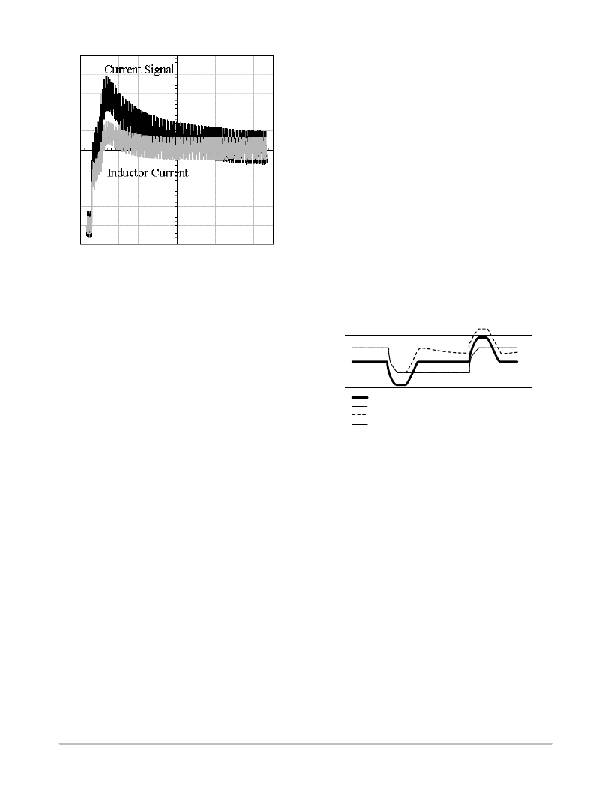
�Figure� 20.� Inductive� Sensing� Waveform� During� a�
�Load� Step� with� Fast� RC� Time� Constant� (50� μ� s/div)�
�The� waveforms� in� Figure� 20� show� a� simulation� of� the�
�current� sense� signal� and� the� actual� inductor� current� during� a�
�positive� step� in� load� current� with� values� of� L� =� 500� nH,�
�R� L� =� 1.6� m� Ω� ,� R� CSx� =� 20� k� Ω� and� C� CSx� =� .01� m� F.� In� this� case,�
�ideal� current� signal� compensation� would� require� R� CSx� to� be�
�31� k� Ω� .� Due� to� the� faster� than� ideal� RC� time� constant,� there� is�
�an� overshoot� of� 50%� and� the� overshoot� decays� with� a� 200� m� s�
�time� constant.� With� this� compensation,� the� I� LIM� pin� threshold�
�must� be� set� more� than� 50%� above� the� full� load� current� to� avoid�
�triggering� current� limit� during� a� large� output� load� step.�
�Transient� Response� and� Adaptive� Voltage� Positioning�
�For� applications� with� fast� transient� currents,� the� output�
�filter� is� frequently� sized� larger� than� ripple� currents� require� in�
�order� to� reduce� voltage� excursions� during� load� transients.�
�Adaptive� voltage� positioning� can� reduce� peak?peak� output�
�voltage� deviations� during� load� transients� and� allow� for� a�
�smaller� output� filter.� The� output� voltage� can� be� set� higher�
�than� nominal� at� light� loads� to� reduce� output� voltage� sag�
�when� the� load� current� is� applied.� Similarly,� the� output�
�voltage� can� be� set� lower� than� nominal� during� heavy� loads� to�
�reduce� overshoot� when� the� load� current� is� removed.� For� low�
�current� applications,� a� droop� resistor� can� provide� fast,�
�accurate� adaptive� positioning.� However,� at� high� currents,�
�the� loss� in� a� droop� resistor� becomes� excessive.� For� example,�
�a� 50� A� converter� with� a� 1� m� Ω� resistor� would� provide� a�
�50� mV� change� in� output� voltage� between� no� load� and� full�
�load� and� would� dissipate� 2.5� W.�
�Lossless� adaptive� voltage� positioning� (AVP)� is� an�
�alternative� to� using� a� droop� resistor,� but� it� must� respond� to�
�changes� in� load� current.� Figure� 21� shows� how� AVP� works.�
�The� waveform� labeled� “normal”� shows� a� converter� without�
�AVP.� On� the� left,� the� output� voltage� sags� when� the� output�
�current� is� stepped� up� and� later� overshoots� when� current� is�
�stepped� back� down.� With� fast� (ideal)� AVP,� the� peak?to?peak�
�excursions� are� cut� in� half.� In� the� slow� AVP� waveform,� the�
�transition� between� fast� and� slow� positioning� is� controlled� by�
�the� total� ramp� size� and� the� error� amp� compensation.� If� the�
�ramp� size� is� too� large� or� the� error� amp� too� slow,� there� will� be�
�a� long� transition� to� the� final� voltage� after� a� transient.� This�
�will� be� most� apparent� with� low� capacitance� output� filters.�
�Normal�
�Fast� Adaptive� Positioning�
�Slow� Adaptive� Positioning�
�Limits�
�Figure� 21.� Adaptive� Voltage� Positioning�
�Overvoltage� Protection�
�Overvoltage� protection� (OVP)� is� provided� as� a� result� of�
�the� normal� operation� of� the� Enhanced� V� 2� control� topology�
�with� synchronous� rectifiers.� The� control� loop� responds� to� an�
�overvoltage� condition� within� 40� ns,� causing� the� GATEx�
�output� to� shut� off.� The� (external)� MOSFET� driver� should�
�react� normally� to� turn� off� the� top� MOSFET� and� turn� on� the�
�bottom� MOSFET.� This� results� in� a� “crowbar”� action� to�
�clamp� the� output� voltage� and� prevent� damage� to� the� load.�
�The� regulator� will� remain� in� this� state� until� the� fault� latch� is�
�reset� by� cycling� power� at� the� V� CC� pin.�
�Power� Good�
�According� to� the� latest� specifications,� the� Power� Good�
�(PWRGD)� signal� must� be� asserted� when� the� output� voltage�
�is� within� a� window� defined� by� the� VID� code,� as� shown� in�
�Figure� 22.�
�The� PWRLS� pin� is� provided� to� allow� the� PWRGD�
�comparators� to� accurately� sense� the� output� voltage.� The�
�effect� of� the� PWRGD� lower� threshold� can� be� modified� using�
�a� resistor� divider� from� the� output� to� PWRLS� to� ground,� as�
�shown� in� Figure� 23.�
�http://onsemi.com�
�16�
�相关PDF资料 |
PDF描述 |
|---|---|
| X4323S8-4.5A | IC SUPERVISOR CPU 32K EE 8-SOIC |
| EMC31DREF-S13 | CONN EDGECARD 62POS .100 EXTEND |
| RBM43DCSI | CONN EDGECARD 86POS DIP .156 SLD |
| P1812R-224K | INDUCTOR POWER 220UH SMD |
| X4323S8-2.7A | IC SUPERVISOR CPU 32K EE 8-SOIC |
相关代理商/技术参数 |
参数描述 |
|---|---|
| NCP5316 | 制造商:ONSEMI 制造商全称:ON Semiconductor 功能描述:Four/Five/Six−Phase Buck CPU Controller |
| NCP5316/D | 制造商:ONSEMI 制造商全称:ON Semiconductor 功能描述:Four/Five/Six-Phase Buck CPU Controller |
| NCP5316_06 | 制造商:ONSEMI 制造商全称:ON Semiconductor 功能描述:Four/Five/Six−Phase Buck CPU Controller |
| NCP5316FTR2 | 功能描述:IC CTRLR BUCK CPU 4/5/6PH 48LQFP RoHS:否 类别:集成电路 (IC) >> PMIC - 稳压器 - 专用型 系列:- 产品培训模块:Lead (SnPb) Finish for COTS Obsolescence Mitigation Program 标准包装:2,000 系列:- 应用:电源,ICERA E400,E450 输入电压:4.1 V ~ 5.5 V 输出数:10 输出电压:可编程 工作温度:-40°C ~ 85°C 安装类型:表面贴装 封装/外壳:42-WFBGA,WLCSP 供应商设备封装:42-WLP 包装:带卷 (TR) |
| NCP5316MNR2 | 功能描述:IC CTRLR BUCK CPU 4/5/6PH 48QFN RoHS:否 类别:集成电路 (IC) >> PMIC - 稳压器 - 专用型 系列:- 产品培训模块:Lead (SnPb) Finish for COTS Obsolescence Mitigation Program 标准包装:2,000 系列:- 应用:电源,ICERA E400,E450 输入电压:4.1 V ~ 5.5 V 输出数:10 输出电压:可编程 工作温度:-40°C ~ 85°C 安装类型:表面贴装 封装/外壳:42-WFBGA,WLCSP 供应商设备封装:42-WLP 包装:带卷 (TR) |
发布紧急采购,3分钟左右您将得到回复。