- 您现在的位置:买卖IC网 > Datasheet目录484 > NOIL1SE3000A-GDC (ON Semiconductor)IC IMAGE SENSOR 3MP 369-PGA Datasheet资料下载
参数资料
| 型号: | NOIL1SE3000A-GDC |
| 厂商: | ON Semiconductor |
| 文件页数: | 14/57页 |
| 文件大小: | 0K |
| 描述: | IC IMAGE SENSOR 3MP 369-PGA |
| 标准包装: | 1 |
| 系列: | * |
| 象素大小: | 8µm x 8µm |
| 有源象素阵列: | 1696H x 1710V |
| 每秒帧数: | 485 |
| 电源电压: | 2.5V, 3.3V |
| 类型: | CMOS 成像 |
| 封装/外壳: | * |
| 供应商设备封装: | * |
| 包装: | * |
| 其它名称: | CYIL1SE3000AA-GZDC CYIL1SE3000AA-GZDC-ND |
第1页第2页第3页第4页第5页第6页第7页第8页第9页第10页第11页第12页第13页当前第14页第15页第16页第17页第18页第19页第20页第21页第22页第23页第24页第25页第26页第27页第28页第29页第30页第31页第32页第33页第34页第35页第36页第37页第38页第39页第40页第41页第42页第43页第44页第45页第46页第47页第48页第49页第50页第51页第52页第53页第54页第55页第56页第57页
�� �
�
�NOIL1SN3000A�
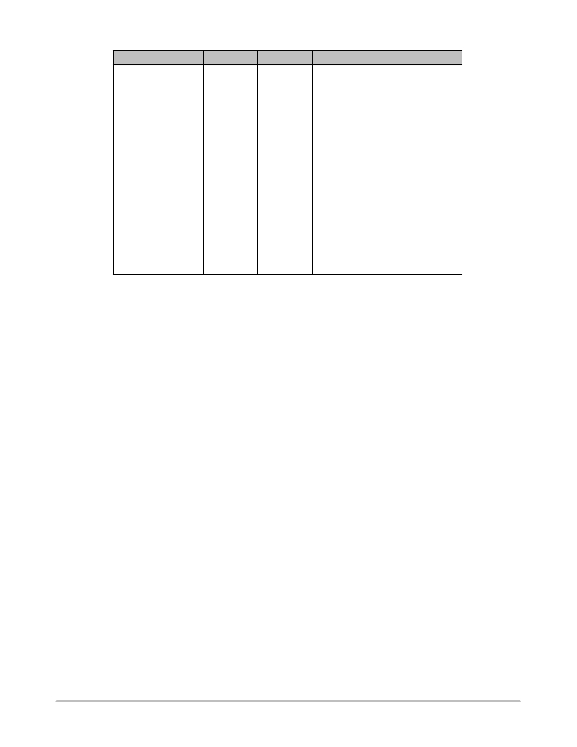
�REG� 72� <� 3:0>�
�0000�
�0001�
�0010�
�0011�
�0100�
�0101�
�0110�
�0111�
�1000�
�1001�
�1010�
�1011�
�1100�
�1101�
�1110�
�1111�
�I� OUT� [mA]�
�1.26�
�1.68�
�2.1�
�2.52�
�2.94�
�3.36�
�3.78�
�4.2�
�4.62�
�5.04�
�5.46�
�5.88�
�6.3�
�6.72�
�7.14�
�7.56�
�RT[?� ]�
�100�
�100�
�100�
�100�
�100�
�100�
�100�
�100�
�72.97�
�68.75�
�68.75�
�68.75�
�50�
�50�
�50�
�50�
�V� OUT� [mV]�
�126�
�168�
�210�
�252�
�294�
�336�
�378�
�420�
�337�
�347�
�375�
�404�
�315�
�336�
�357�
�378�
�Co� mment� s�
�Low� power� range�
�Standard� range�
�Extra� drive� current�
�to� accommodate� high�
�Interconnect� capacitance�
�Figure� 13.� LVDS� Driver� Programmable� Drive� Current� Settings�
�LVDS� Sync� Channel�
�LUPA3000� includes� a� LVDS� output� channel� to� encode�
�sensor� synchronization� control� words� such� as� start� of� frame�
�(SOF),� start� of� line� (SOL),� end� of� line� (EOL),� idle� words�
�(IdleA� and� IdleB),� and� the� sensor� line� address.�
�This� channel� includes� a� serializer� logic� section,� but�
�receives� its� input� directly� from� the� image� core� sequencer.� An�
�additional� synchronization� control� logic� block� ensures�
�proper� data� alignment� of� the� synchronization� codes� to�
�account� for� the� latency� incurred� in� the� other� 32� data� channels�
�(due� to� AFE� and� ADC� signal� processing).� The� LVDS� output�
�driver� is� similar� to� that� used� in� other� data� channel� outputs.�
�LVDS� Clk� (Clock)� Output�
�The� LUPA3000� provides� a� LVDS� clock� output� channel.�
�This� channel� provides� an� output� clock� that� is� in� phase� and�
�aligned� with� the� data� bit� stream� of� the� 32� data� channels.� It� is�
�required� for� clock� and� data� recovery� by� the� system�
�processing� circuits.�
�A� serializer� logic� section� is� connected� to� accept� the�
�differential� CMOS� serializer� clock,� after� processing� through�
�the� clock� distribution� buffer� network� that� provides� clocks� to�
�all� LUPA3000� data� channels.� The� group� delay� of� the� output�
�clock� and� data� channels� is� ~2.5� ns� relative� to� the� incoming�
�master� clock.� The� LVDS� output� driver� is� similar� to� that� used�
�in� other� data� channel� outputs.�
�LVDS� CLK� (Clock)� Input�
�LUPA3000� includes� a� differential� LVDS� receiver� for� the�
�master� input� clock.� The� input� clock� rate� is� typically�
�206� MHz� and� also� complies� with� the� ANSI� LVDS� receiver�
�standards.� The� input� clock� drives� the� internal� clock�
�generator� circuit� that� produces� the� required� internal� clocks�
�for� image� core� and� sequencer,� AFE� and� ADCs,� CRC�
�insertion� logic,� and� serializers.� LUPA3000� requires� the�
�following� internal� clock� domains� (all� internal� clock� domains�
�are� 2.5� V� CMOS� levels):�
�?� Serializer� clock� =� 1x� differential� version� of� the� input�
�clock� (206� MHz� typical)�
�?� CRC� clock� =� 1/4x� the� input� clock� (51.5� MHz� typical)�
�?� Load� pulse� =� 1/4� (the� input� clock)at� 12.5%� duty� cycle�
�version� of� the� input� clock:� for� load� and� handshake�
�between� CRC� parallel� data� to� serializer�
�?� ADC� and� AFE� clock� =� 1/8x� the� input� clock�
�(25.75� MHz� typical)�
�?� Sensor� clock� =� 1/4x� the� input� clock� (51.5� MHz� typical)�
�with� programmable� delay�
�?� ADC� clock� =1/8x� the� input� clock� (25.75� MHz� typical)�
�with� programmable� delay�
�All� clock� domains� are� designed� with� identical� clock� buffer�
�networks� to� ensure� equal� group� delays� and� maintain� less�
�than� 100� ps� maximum� channel� to� channel� clock� variation.�
�Programmable� delay� adjustment� is� provided� for� the� clock�
�domains� of� image� sensor� core� and� sequencer.� This�
�adjustment� optimizes� the� data� acquisition� handshaking�
�between� the� image� sensor� core� and� the� digitization� and�
�serialization� channels.� SPI� register� 65� (decimal)� controls�
�delay� (or� advance)� adjustments� for� these� two� clocks.� For�
�each� of� these� two� imager� clocks,� 15� adjustments� settings� are�
�provided.� Each� setting� allows� adjustment� for� 1/(2x� master�
�clock)� adjustment.� For� example,� if� the� master� input� clock�
�runs� at� 206� MHz,� 1/412� MHz� =� 2.41� ns� adjustment�
�resolution� is� possible.� Refer� to� Sensor� Clock� Edge� Adjust�
�Register� (b1000001� /� d65)� on� page� 26� for� programming�
�details.�
�ON� Semiconductor� provides� default� settings� for� the�
�programmable� delay.� These� settings� allow� correct�
�http://onsemi.com�
�14�
�相关PDF资料 |
PDF描述 |
|---|---|
| NOIL1SM0300A-WWC | IC IMAGE SENSOR LUPA300 48LLC |
| NOIL2SC1300A-GDC | IC IMAGE SENSOR LUPA1300 168PGA |
| NOIV1SE025KA-GDC | IC IMAGE SENSOR 25MP 355PGA |
| NP100P04PDG-E1-AY | MOSFET P-CH -40V MP-25ZP/TO-263 |
| NP100P04PLG-E1-AY | MOSFET P-CH -40V MP-25ZP/TO-263 |
相关代理商/技术参数 |
参数描述 |
|---|---|
| NOIL1SM0300A-QDC | 功能描述:IC IMAGE SENSOR LUPA300 48LLC RoHS:是 类别:传感器,转换器 >> 图像,相机 系列:* 标准包装:480 系列:- 象素大小:6.7µm x 6.7µm 有源象素阵列:768H x 488V 每秒帧数:52 电源电压:3.3V 类型:CMOS 成像 封装/外壳:48-QFP 供应商设备封装:48-QFP 包装:托盘 请注意:* 配用:4H2105-ND - HEADBOARD FOR KAC-004014H2104-ND - KIT EVAL FOR KAC-00401 其它名称:4H20954H2095-NDKAC-00401-CBC-LB-A0 |
| NOIL1SM0300A-WWC | 功能描述:IC IMAGE SENSOR LUPA300 48LLC RoHS:是 类别:传感器,转换器 >> 图像,相机 系列:LUPA300 标准包装:480 系列:- 象素大小:6.7µm x 6.7µm 有源象素阵列:768H x 488V 每秒帧数:52 电源电压:3.3V 类型:CMOS 成像 封装/外壳:48-QFP 供应商设备封装:48-QFP 包装:托盘 请注意:* 配用:4H2105-ND - HEADBOARD FOR KAC-004014H2104-ND - KIT EVAL FOR KAC-00401 其它名称:4H20954H2095-NDKAC-00401-CBC-LB-A0 |
| NOIL1SM1300AWES | 制造商:ON Semiconductor 功能描述:PW/H |
| NOIL1SM4000A | 制造商:ONSEMI 制造商全称:ON Semiconductor 功能描述:LUPA4000: 4 MegaPixel High Speed CMOS Sensor |
| NOIL1SM4000A-GDC | 功能描述:IC IMAGE SENSOR LUPA4000 127PGA RoHS:是 类别:传感器,转换器 >> 图像,相机 系列:* 标准包装:480 系列:- 象素大小:6.7µm x 6.7µm 有源象素阵列:768H x 488V 每秒帧数:52 电源电压:3.3V 类型:CMOS 成像 封装/外壳:48-QFP 供应商设备封装:48-QFP 包装:托盘 请注意:* 配用:4H2105-ND - HEADBOARD FOR KAC-004014H2104-ND - KIT EVAL FOR KAC-00401 其它名称:4H20954H2095-NDKAC-00401-CBC-LB-A0 |
发布紧急采购,3分钟左右您将得到回复。