- 您现在的位置:买卖IC网 > Datasheet目录484 > NOIV1SE025KA-GDC (ON Semiconductor)IC IMAGE SENSOR 25MP 355PGA Datasheet资料下载
参数资料
| 型号: | NOIV1SE025KA-GDC |
| 厂商: | ON Semiconductor |
| 文件页数: | 10/76页 |
| 文件大小: | 0K |
| 描述: | IC IMAGE SENSOR 25MP 355PGA |
| 标准包装: | 14 |
| 系列: | * |
| 象素大小: | 4.5µm x 4.5µm |
| 有源象素阵列: | 5120H x 5120V |
| 每秒帧数: | 53 |
| 类型: | CMOS 成像 |
| 封装/外壳: | * |
| 供应商设备封装: | * |
| 包装: | * |
第1页第2页第3页第4页第5页第6页第7页第8页第9页当前第10页第11页第12页第13页第14页第15页第16页第17页第18页第19页第20页第21页第22页第23页第24页第25页第26页第27页第28页第29页第30页第31页第32页第33页第34页第35页第36页第37页第38页第39页第40页第41页第42页第43页第44页第45页第46页第47页第48页第49页第50页第51页第52页第53页第54页第55页第56页第57页第58页第59页第60页第61页第62页第63页第64页第65页第66页第67页第68页第69页第70页第71页第72页第73页第74页第75页第76页
��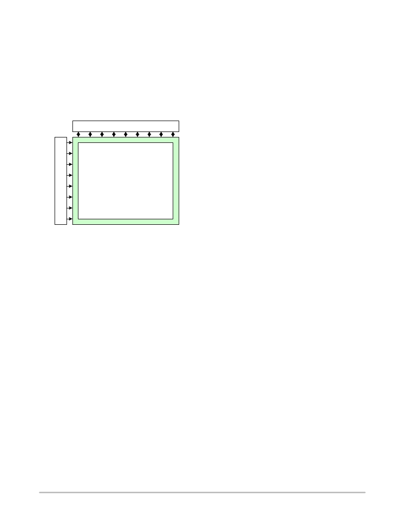 �
�
�NOIV1SN025KA�
�array� in� global� shutter� mode� with� DS,� or� rolling� shutter� mode�
�with� CDS.�
�The� function� of� the� row� drivers� is� to� access� the� image� array�
�line� by� line,� or� all� lines� together,� to� reset� or� read� the� pixel�
�data.� The� row� drivers� are� controlled� by� the� on-chip�
�sequencer� and� can� access� the� pixel� array� in� global� and� rolling�
�shutter� modes.�
�The� pixel� biasing� block� guarantees� that� the� data� on� a� pixel�
�is� transferred� properly� to� the� column� multiplexer� when� the�
�row� drivers� select� a� pixel� line� for� readout.�
�Pixel� Biasing�
�4� Dummy� rows�
�Pixel� Array�
�5120� (X)� x� 5120� (Y)�
�Analog� Front� End�
�The� AFE� contains� 64� channels,� each� containing� a� PGA�
�and� a� 10-bit� ADC.� The� PGA� can� be� programmed� to� apply� a�
�gain� of� 1x,� 1.39x,� 1.94x,� and� 2.72x� to� the� image� signal.�
�Together� with� the� gain� applied� in� the� column� multiplexer,� a�
�total� signal� gain� of� 10x� can� be� achieved.�
�For� each� of� the� 64� channels,� a� pipelined� 10-bit� ADC� is�
�used� to� convert� the� analog� image� data� into� a� digital� signal,�
�which� is� delivered� to� the� data� formatting� block.� A� black�
�calibration� loop� is� implemented� to� ensure� that� the� black� level�
�is� mapped� to� match� the� correct� ADC� input� level.�
�Data� Formatting�
�The� data� block� receives� data� from� two� ADCs� and�
�multiplexes� this� data� to� one� LVDS� block.� A� cyclic�
�redundancy� check� (CRC)� code� is� calculated� on� the� passing�
�data.� For� each� LVDS� output� channel,� one� data� block� is�
�instantiated.� An� extra� data� block� is� foreseen� to� transmit�
�synchronization� codes� such� as� frame� start,� line� start,� frame�
�end,� and� line� end� indications.�
�The� data� block� calculates� a� CRC� once� per� line� for� every�
�channel.� This� CRC� code� can� be� used� for� error� detection� at� the�
�receiving� end.�
�+pixel(0;0)�
�4� Dummy� rows�
�Serializer� and� LVDS� Interface�
�Figure� 6.� Image� Core� Diagram�
�LVDS� Clock� Receiver�
�The� LVDS� clock� receiver� receives� an� LVDS� clock� signal�
�and� distributes� the� required� clocks� to� the� sensor.�
�Typical� input� clock� frequency� is� 310� MHz� in� 10-bit� mode�
�and� 248� MHz� in� 8-bit� mode.� The� clock� input� needs� to� be�
�terminated� with� a� 100� W� resistor.�
�Column� Multiplexer�
�The� 5120� pixels� of� one� image� row� are� stored� in� 5120�
�column� sample-and-hold� (S/H)� stages.� These� stages� store�
�both� the� reset� and� integrated� signal� levels.�
�The� data� stored� in� the� column� S/H� stages� is� read� out�
�through� 64� parallel� differential� outputs� operating� at� a�
�frequency� of� 31� MHz.�
�At� this� stage,� the� reset� signal� and� integrated� signal� values�
�are� transferred� into� an� FPN-corrected� differential� signal.� A�
�programmable� gain� of� 1x,� 2x,� or� 4x� can� be� applied� to� the�
�signal� at� this� stage.� The� column� multiplexer� also� supports� a�
�subsampled� readout� mode� (read-1-skip-1� for� mono� and�
�read-2-skip-2� for� color� version).� Enabling� this� mode� can�
�speed� up� the� frame� rate,� with� a� decrease� in� resolution.�
�The� serializer� and� LVDS� interface� block� receives� the�
�formatted� (10-bit� or� 8-bit)� data� from� the� data� formatting�
�block.� This� data� is� serialized� and� transmitted� by� the� LVDS�
�output� driver.�
�In� 10-bit� mode,� the� maximum� output� data� bit� rate� is�
�620� Mbps� per� channel.� In� 8-bit� mode,� the� maximum� output�
�data� bit� rate� is� 496� Mbps� per� channel.�
�In� addition� to� the� 32� LVDS� data� outputs,� two� extra� LVDS�
�outputs� are� available.� One� of� these� outputs� carries� the� output�
�clock,� which� is� skew� aligned� to� the� output� data� channels.� The�
�second� LVDS� output� contains� frame� format� synchronization�
�codes� to� serve� system-level� image� reconstruction.�
�Sequencer�
�The� sequencer� is� responsible� for� the� following� tasks:�
�?� Controls� the� image� core.� Starts� and� stops� integration� in�
�rolling� and� global� shutter� modes� and� control� pixel�
�readout.�
�?� Operates� the� sensor� in� master� or� slave� mode.�
�?� Applies� the� window� settings.� Organizes� readouts� so� that�
�only� the� configured� windows� are� read.�
�?� Controls� the� column� multiplexer� and� analog� core.�
�Applies� gain� settings� and� subsampling� modes� at� the�
�Bias� Generator�
�The� bias� generator� generates� all� required� reference�
�voltages� and� bias� currents� that� the� on-chip� blocks� use.� An�
�?�
�correct� time,� without� corrupting� image� data.�
�Starts� up� the� sensor� correctly� when� leaving� standby�
�mode.�
�external� resistor� of� 47� k� W� ,� connected� between� the� pins�
�ibias_master� and� gnda_33� is� required� for� the� bias� generator�
�to� operate� properly.�
�http://onsemi.com�
�10�
�相关PDF资料 |
PDF描述 |
|---|---|
| NP100P04PDG-E1-AY | MOSFET P-CH -40V MP-25ZP/TO-263 |
| NP100P04PLG-E1-AY | MOSFET P-CH -40V MP-25ZP/TO-263 |
| NP100P06PDG-E1-AY | MOSFET P-CH -60V MP-25ZP/TO-263 |
| NP100P06PLG-E1-AY | MOSFET P-CH -60V MP-25ZP/TO-263 |
| NP109N04PUJ-E1B-AY | MOSFET N-CH 40V MP-25ZP/TO-263 |
相关代理商/技术参数 |
参数描述 |
|---|---|
| NOIV1SE1300A-QDC | 功能描述:图像传感器和彩色传感器 VITA 1300 1.3 Mpx 150FPS Globl Shutter RoHS:否 制造商:Avago Technologies 类型:Color Sensors 工作电源电压:2.5 V 封装 / 箱体: 图象大小: 颜色读出:Color 最大工作温度:+ 70 C 最小工作温度:- 25 C 封装:Reel |
| NOIV1SE1300A-QXC | 制造商:ONSEMI 制造商全称:ON Semiconductor 功能描述:VITA 1300 1.3 Megapixel 150 FPS Global Shutter CMOS Image Sensor |
| NOIV1SE1300A-XDC | 制造商:ONSEMI 制造商全称:ON Semiconductor 功能描述:VITA 1300 1.3 Megapixel 150 FPS Global Shutter CMOS Image Sensor |
| NOIV1SE1300A-XXC | 制造商:ONSEMI 制造商全称:ON Semiconductor 功能描述:VITA 1300 1.3 Megapixel 150 FPS Global Shutter CMOS Image Sensor |
| NOIV1SE2000A-QDC | 功能描述:IC IMAGE SENSOR 2.3MP 52LLC RoHS:是 类别:传感器,转换器 >> 图像,相机 系列:* 标准包装:480 系列:- 象素大小:6.7µm x 6.7µm 有源象素阵列:768H x 488V 每秒帧数:52 电源电压:3.3V 类型:CMOS 成像 封装/外壳:48-QFP 供应商设备封装:48-QFP 包装:托盘 请注意:* 配用:4H2105-ND - HEADBOARD FOR KAC-004014H2104-ND - KIT EVAL FOR KAC-00401 其它名称:4H20954H2095-NDKAC-00401-CBC-LB-A0 |
发布紧急采购,3分钟左右您将得到回复。