- 您现在的位置:买卖IC网 > Datasheet目录484 > NOIV1SE025KA-GDC (ON Semiconductor)IC IMAGE SENSOR 25MP 355PGA Datasheet资料下载
参数资料
| 型号: | NOIV1SE025KA-GDC |
| 厂商: | ON Semiconductor |
| 文件页数: | 9/76页 |
| 文件大小: | 0K |
| 描述: | IC IMAGE SENSOR 25MP 355PGA |
| 标准包装: | 14 |
| 系列: | * |
| 象素大小: | 4.5µm x 4.5µm |
| 有源象素阵列: | 5120H x 5120V |
| 每秒帧数: | 53 |
| 类型: | CMOS 成像 |
| 封装/外壳: | * |
| 供应商设备封装: | * |
| 包装: | * |
第1页第2页第3页第4页第5页第6页第7页第8页当前第9页第10页第11页第12页第13页第14页第15页第16页第17页第18页第19页第20页第21页第22页第23页第24页第25页第26页第27页第28页第29页第30页第31页第32页第33页第34页第35页第36页第37页第38页第39页第40页第41页第42页第43页第44页第45页第46页第47页第48页第49页第50页第51页第52页第53页第54页第55页第56页第57页第58页第59页第60页第61页第62页第63页第64页第65页第66页第67页第68页第69页第70页第71页第72页第73页第74页第75页第76页
�� �
�
�NOIV1SN025KA�
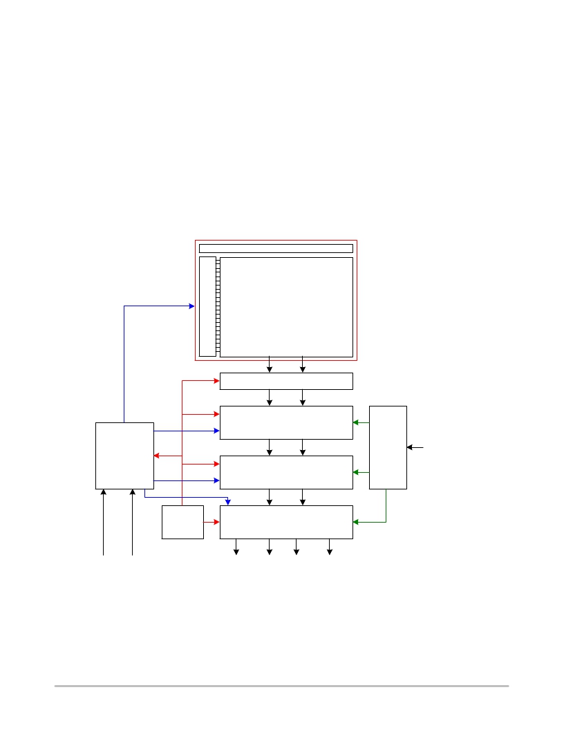
�OVERVIEW�
�Figure� 5� gives� an� overview� of� all� functional� blocks� in� the�
�image� sensor.� The� system� clock� is� received� by� the� LVDS�
�clock� receiver� block� and� distributed� to� other� blocks.� The�
�sequencer� defines� the� sensor� timing� and� controls� the� image�
�core.� The� sequencer� is� started� either� autonomously� (master�
�mode)� or� on� assertion� of� an� external� trigger� (slave� mode).�
�The� image� core� contains� all� pixels� and� readout� circuits.� The�
�column� structure� selects� pixels� for� readout� and� performs�
�correlated� double� sampling� (CDS)� or� double� sampling� (DS).�
�The� data� comes� out� sequentially� and� is� fed� into� the� analog�
�front� end� (AFE)� block.� The� programmable� gain� amplifier�
�(PGA)� of� the� AFE� adds� the� offset� and� gain.� The� output� is� a�
�fully� differential� analog� signal� that� goes� to� the� ADC,� where�
�Depending� on� the� operating� mode,� eight� or� ten� bits� are� fed�
�into� the� data� formatting� block.� This� block� adds�
�synchronization� information� to� the� data� stream� based� on� the�
�frame� timing.� The� data� then� goes� to� the� low� voltage� serial�
�(LVDS)� interface� block� that� sends� the� data� out� through� the�
�I/O� ring.�
�On-chip� programmability� is� controlled� through� the� Serial�
�Peripheral� Interface� (SPI).� See� Register� Map� on� page� 43� for�
�register� details.� A� bias� block� generates� bias� currents� and�
�voltages� for� all� analog� blocks� on� the� chip.� By� controlling� the�
�bias� current,� the� speed-versus-power� of� each� block� can� be�
�tuned.� All� biasing� programmability� is� contained� in� the� bias�
�block.�
�the� analog� signal� is� converted� to� a� 10-bit� data� stream.�
�Image� Core�
�Image� Core� Bias�
�Pixel� Array�
�(5120� x� 5120)�
�Column� Structure�
�64� Analog� Channels�
�Analog� Front� End� (AFE)�
�64� x� 10� bit�
�Biasing� and�
�External�
�Control� and�
�Digital� Channels�
�Bandgap�
�Resistor�
�Registers�
�Data� Formatting�
�32� x� 10-bit�
�Digital� Channels�
�LVDS� Clock�
�Receiver�
�Serializers� &� LVDS� Interface�
�32� LVDS� Channels�
�1� LVDS� Sync� Channel�
�SPI�
�Interface�
�Reset�
�LVDS� Outputs/Parallel� Outputs�
�1� LVDS� Clock� Channel�
�Figure� 5.� Block� Diagram�
�Image� Core�
�The� image� core� consists� of:�
�?� Pixel� array�
�?� Address� decoders� and� row� drivers�
�?� Pixel� biasing�
�The� pixel� array� contains� 5120� x� 5120� readable� pixels� with�
�a� pixel� pitch� of� 4.5� m� m.� Four� dummy� pixel� rows� and� columns�
�are� placed� at� every� side� of� the� pixel� array� to� eliminate�
�possible� edge� effects.� The� sensor� uses� a� 5T� pixel�
�architecture,� which� makes� it� possible� to� read� out� the� pixel�
�http://onsemi.com�
�9�
�相关PDF资料 |
PDF描述 |
|---|---|
| NP100P04PDG-E1-AY | MOSFET P-CH -40V MP-25ZP/TO-263 |
| NP100P04PLG-E1-AY | MOSFET P-CH -40V MP-25ZP/TO-263 |
| NP100P06PDG-E1-AY | MOSFET P-CH -60V MP-25ZP/TO-263 |
| NP100P06PLG-E1-AY | MOSFET P-CH -60V MP-25ZP/TO-263 |
| NP109N04PUJ-E1B-AY | MOSFET N-CH 40V MP-25ZP/TO-263 |
相关代理商/技术参数 |
参数描述 |
|---|---|
| NOIV1SE1300A-QDC | 功能描述:图像传感器和彩色传感器 VITA 1300 1.3 Mpx 150FPS Globl Shutter RoHS:否 制造商:Avago Technologies 类型:Color Sensors 工作电源电压:2.5 V 封装 / 箱体: 图象大小: 颜色读出:Color 最大工作温度:+ 70 C 最小工作温度:- 25 C 封装:Reel |
| NOIV1SE1300A-QXC | 制造商:ONSEMI 制造商全称:ON Semiconductor 功能描述:VITA 1300 1.3 Megapixel 150 FPS Global Shutter CMOS Image Sensor |
| NOIV1SE1300A-XDC | 制造商:ONSEMI 制造商全称:ON Semiconductor 功能描述:VITA 1300 1.3 Megapixel 150 FPS Global Shutter CMOS Image Sensor |
| NOIV1SE1300A-XXC | 制造商:ONSEMI 制造商全称:ON Semiconductor 功能描述:VITA 1300 1.3 Megapixel 150 FPS Global Shutter CMOS Image Sensor |
| NOIV1SE2000A-QDC | 功能描述:IC IMAGE SENSOR 2.3MP 52LLC RoHS:是 类别:传感器,转换器 >> 图像,相机 系列:* 标准包装:480 系列:- 象素大小:6.7µm x 6.7µm 有源象素阵列:768H x 488V 每秒帧数:52 电源电压:3.3V 类型:CMOS 成像 封装/外壳:48-QFP 供应商设备封装:48-QFP 包装:托盘 请注意:* 配用:4H2105-ND - HEADBOARD FOR KAC-004014H2104-ND - KIT EVAL FOR KAC-00401 其它名称:4H20954H2095-NDKAC-00401-CBC-LB-A0 |
发布紧急采购,3分钟左右您将得到回复。