- 您现在的位置:买卖IC网 > PDF目录189259 > NT2GT72U4PD0BV-3C (NANYA TECHNOLOGY CORP) 256M X 72 DDR DRAM MODULE, 0.45 ns, DMA240 PDF资料下载
参数资料
| 型号: | NT2GT72U4PD0BV-3C |
| 厂商: | NANYA TECHNOLOGY CORP |
| 元件分类: | DRAM |
| 英文描述: | 256M X 72 DDR DRAM MODULE, 0.45 ns, DMA240 |
| 封装: | ROHS COMPLIANT, DIMM-240 |
| 文件页数: | 7/27页 |
| 文件大小: | 648K |
| 代理商: | NT2GT72U4PD0BV-3C |
第1页第2页第3页第4页第5页第6页当前第7页第8页第9页第10页第11页第12页第13页第14页第15页第16页第17页第18页第19页第20页第21页第22页第23页第24页第25页第26页第27页
NT1GT72U89D0BV / NT2GT72U4PD0BV / NT4GT72U4ND0BV
NT2GT72U8PD0BV
1GB: 128M x 72 / 2GB: 256M x 72 / 4GB: 512M x 72
PC2-5300 / PC3-6400
Registered DDR2 SDRAM DIMM
REV 1.1
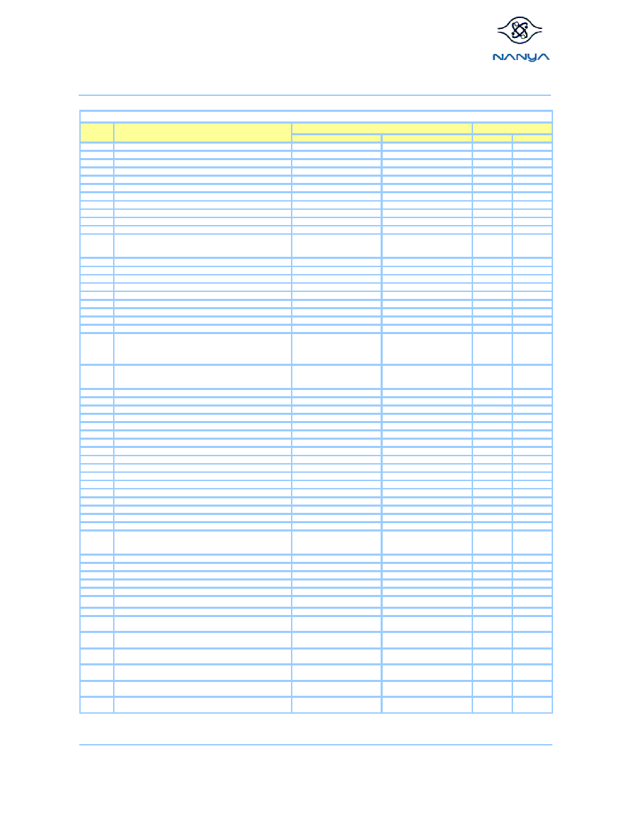
15
01/2009
NANYA TECHNOLOGY CORP.
NANYA TECHNOLOGY CORP. reserves the right to change Products and Specifications without notice.
-3C
-AD
-3C
-AD
0
Number of Serial PD Bytes Written during Production
128
80
1
Total Number of Bytes in Serial PD device
256
08
2
Fundamental Memory Type
DDR2 SDRAM
08
3
Number of Row Addresses on Assembly
14
0E
4
Number of Column Addresses on Assembly
11
0B
5
Number of DIMM Ranks
Module Height = 30.0mm, 2
ranks
Module Height = 30.0mm, 2
ranks
61
6
Data Width of Assembly
X72
48
7
Reserved
Undefined
00
8
Voltage Interface Level of this Assembly
SSTL 1.8V
05
9
DDR2 SDRAM Device Cycle Time at CL=X
3ns
2.5ns
30
25
10
DDR2 SDRAM Device Access Time from Clock at CL=X
0.45ns
0.4ns
45
40
11
DIMM Configuration Type
Address/Command Parity,
Data ECC,
Non Data Parity,
Address/Command Parity,
Data ECC,
Non Data Parity,
06
12
Refresh Rate/Type
7.8 As
82
13
Primary DDR2 SDRAM Width
X4
04
14
Error Checking DDR2 SDRAM Device Width
X4
04
15
Reserved
Undefined
00
16
DDR2 SDRAM Device Attributes: Burst Length Supported
4,8
0C
17
DDR2 SDRAM Device Attributes: Number of Device Banks
8
08
18
DDR2 SDRAM Device Attributes: CAS Latencies Supported
3,4,5
4,5,6
38
70
19
DIMM Mechanical Characteristics
x B 4.10 (mm)
01
20
DDR2 SDRAM DIMM Type Information
RDIMM (133.35mm)
01
21
DDR2 SDRAM Module Attributes:
Analysis probe installed : No,
FET Switch External Enable : No,
Number of PLLs : 1,
Number of Active Registers : 4,
Analysis probe installed : No,
FET Switch External Enable : No,
Number of PLLs : 1,
Number of Active Registers : 4,
07
22
DDR2 SDRAM Device Attributes: General
Supports Weak Driver,
Supports 50 ohm ODT,
Supports PASR,
Supports Weak Driver,
Supports 50 ohm ODT,
Supports PASR,
07
23
Minimum Clock Cycle at CL=X-1
3.75ns
3ns
3D
30
24
Maximum Data Access Time from Clock at CL=X-1
0.5ns
0.45ns
50
45
25
Minimum Clock Cycle Time at CL=X-2
5ns
3.75ns
50
3D
26
Maximum Data Access Time from Clock at CL=X-2
0.6ns
0.5ns
60
50
27
Minimum Row Precharge Time (tRP)
15ns
3C
28
Minimum Row Active to Row Active delay (tRRD)
7.5ns
1E
29
Minimum RAS to CAS delay (tRCD)
15ns
3C
30
Minimum RAS Pulse Width (tRAS)
45ns
2D
31
Module Bank Density
2GB
02
32
Address and Command Setup Time Before Clock (tIS)
0.2ns
0.17ns
20
17
33
Address and Command Hold Time After Clock (tIH)
0.27ns
0.25ns
27
25
34
Data Input Setup Time Before Clock (tDS)
0.1ns
0.05ns
10
05
35
Data Input Hold Time After Clock (tDH)
0.17ns
0.12ns
17
12
36
Write Recovery Time (tWR)
15ns
3C
37
Internal Write to Read Command delay (tWTR)
7.5ns
1E
38
Internal Read to Precharge delay (tRTP)
7.5ns
1E
39
Reserved
Undefined
00
40
Extension of Byte 41 tRC and Byte 42 tRFC
The number below a decimal
point of tRC and tRFC are 0,
tRFC is less than 256ns.
The number below a decimal
point of tRC and tRFC are 0,
tRFC is less than 256ns.
06
41
Minimum Core Cycle Time (tRC)
60ns
3C
42
Min. Auto Refresh Command Cycle Time (tRFC)
127.5ns
7F
43
Maximum Clock Cycle Time (tCK)
8ns
80
44
Max. DQS-DQ Skew Factor (tDQS)
0.24ns
0.2ns
18
14
45
Read Data Hold Skew Factor (tQHS)
0.34ns
0.3ns
22
1E
46
PLL Relock Time
15As
0F
47
Tcasemax, DT4R4W Delta
Undefined
00
48
Thermal Resistance of DRAM Package from Top (Case) to
Ambient (Psi T-A DRAM)
Undefined
00
49
DRAM Case Temperature Rise from Ambient due to Activate-
Precharge/Mode Bits (DT0/Mode Bits)
Undefined
00
50
DRAM Case Temperature Rise from Ambient due to
Precharge/Quiet Standby (DT2N/DT2Q)
Undefined
00
51
DRAM Case Temperature Rise from Ambient due to precharge
Power-Down (DT2P)
Undefined
00
52
DRAM Case Temperature Rise from Ambient due to Active
Standby (DT3N)
Undefined
00
53
DRAM Case Temperature Rise from Ambient due to Active Power-
Down with Fast PDN Exit (DT3P fast)
Undefined
00
Serial PD Data Entry (Hex.)
Serial Presence Detect (Part 1 of 2) [NT4GT72U4ND0BV, 4GB – 2 Ranks, 256Mx4 DDR2 SDRAMs]
Byte
Description
SPD Entry Value
相关PDF资料 |
PDF描述 |
|---|---|
| NT512T64U88B0BY-3C | 64M X 64 DDR DRAM MODULE, 0.5 ns, DMA240 |
| NT56V6620C0T-75 | SYNCHRONOUS DRAM, PDSO54 |
| NT5CB256M4AN-BF | DDR DRAM, PBGA78 |
| NT5DS64M8BF-6KI | DDR DRAM, PBGA60 |
| NT5SE8M16DS-6K | 8M X 16 SYNCHRONOUS DRAM, 5 ns, PDSO54 |
相关代理商/技术参数 |
参数描述 |
|---|---|
| NT2H0301F0DTL,125 | 功能描述:RFID应答器 RoHS:否 制造商:NXP Semiconductors 存储容量: 工作温度范围: 安装风格: 封装 / 箱体: 封装:Reel |
| NT2H0301F0DTP,118 | 制造商:NXP Semiconductors 功能描述:NT2H0301F0DTP - Tape and Reel 制造商:NXP Semiconductors 功能描述:PHANT2H0301F0DTP,118 NFC FORUM TYPE 2 TA 制造商:NXP Semiconductors 功能描述:IC SMART TAG NFC TYPE 2 8HWSON 制造商:NXP Semiconductors 功能描述:NT2H0301F0DTP/HWSON8/REEL13// |
| NT2H0301F0DTP,147 | 制造商:NXP Semiconductors 功能描述:CHIPSET |
| NT2H0301F0DUDV | 制造商:NXP Semiconductors 功能描述:CHIPSET |
| NT2H0301G0DUD,005 | 制造商:NXP Semiconductors 功能描述:NT2H0301G0DUD/UNCASED/FOIL// - Gel-pak, waffle pack, wafer, diced wafer on film 制造商:NXP Semiconductors 功能描述:IC SMART TAG NFC TYPE 2 UNCASED |
发布紧急采购,3分钟左右您将得到回复。