- 您现在的位置:买卖IC网 > PDF目录224604 > NT5TU64M16DG-3C (NANYA TECHNOLOGY CORP) 64M X 16 DDR DRAM, 0.45 ns, PBGA84 PDF资料下载
参数资料
| 型号: | NT5TU64M16DG-3C |
| 厂商: | NANYA TECHNOLOGY CORP |
| 元件分类: | DRAM |
| 英文描述: | 64M X 16 DDR DRAM, 0.45 ns, PBGA84 |
| 封装: | GREEN, BGA-84 |
| 文件页数: | 9/85页 |
| 文件大小: | 2622K |
| 代理商: | NT5TU64M16DG-3C |
第1页第2页第3页第4页第5页第6页第7页第8页当前第9页第10页第11页第12页第13页第14页第15页第16页第17页第18页第19页第20页第21页第22页第23页第24页第25页第26页第27页第28页第29页第30页第31页第32页第33页第34页第35页第36页第37页第38页第39页第40页第41页第42页第43页第44页第45页第46页第47页第48页第49页第50页第51页第52页第53页第54页第55页第56页第57页第58页第59页第60页第61页第62页第63页第64页第65页第66页第67页第68页第69页第70页第71页第72页第73页第74页第75页第76页第77页第78页第79页第80页第81页第82页第83页第84页第85页
NT5TU256M4GE / NT5TU128M8GE / NT5TU64M16GG
1Gb DDR2 SDRAM
17
REV 1.0
06 / 2010
Extended Mode Register Set
–EMRS (1)
The extended mode register EMRS(1) stores the data for enabling or disabling the DLL, output driver strength, additive
latency, ODT,
disable, OCD program, RQDS enable. The default value of the extended mode register EMRS(1) is
not defined, therefore the extended mode register must be written after power-up for proper operation. The extended
mode register is written by asserting low on
, , , , BA1 and high on BA0, while controlling the state of the
address pins. The DDR2 SDRAM should be in all bank precharge with CKE already high prior to writing into the extended
mode register. The mode register set command cycle time (tMRD) must be satisfied to complete the write operation to the
EMRS (1). Mode register contents can be changed using the same command and clock cycle requirements during normal
operation as long as all banks are in precharge state. A0 is used for DLL enable or disable. A1 is used for enabling a half
strength output driver. A3-A5 determines the additive latency, A7-A9 are used for OCD control, A10 is used for
disable and A11 is used for RDQS enable. A2 and A6 are used for ODT setting.
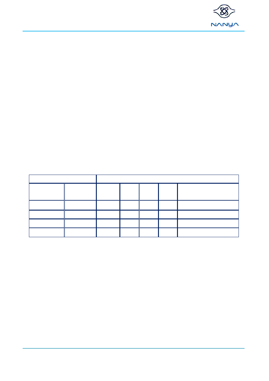
Single-ended and Differential Data Strobe Signals
The following table lists all possible combinations for DQS,
, RDQS, which can be programmed by A10 & A11
address bits in EMRS(1). RDQS and
are available in x8 components only. If RDQS is enabled in x8 components,
the DM function is disabled.
RDQS is active for reads and dont care for writes.
EMRS(1)
Strobe Function Matrix
A11
(RDQS Enable)
A10
(
Enable)
RDQS/DM
DQS
Signaling
0 (Disable)
0 (Enable)
DM
Hi-Z
DQS
differential DQS signals
0 (Disable)
1 (Disable)
DM
Hi-Z
DQS
Hi-Z
single-ended DQS signals
1 (Enable)
0 (Enable)
RDQS
DQS
differential DQS signals
1 (Enable)
1 (Disable)
RDQS
Hi-Z
DQS
Hi-Z
single-ended DQS signals
DLL Enable/Disable
The DLL must be enabled for normal operation. DLL enable is required during power up initialization, and upon returning
to normal operation after having the DLL disabled. The DLL is automatically disabled when entering Self-Refresh
operation and is automatically re-enabled and reset
upon exit of Self-Refresh operation. Any time the DLL is reset,
200 clock cycles must occur before a Read command can be issued to allow time for the internal clock to be
synchronized with the external clock. Less clock cycles may result in a violation of the tAC or tDQSCK
parameters.
Output Disable (Qoff)
Under normal operation, the DRAM outputs are enabled during Read operation for driving data (Qoff bit in the EMRS (1) is
set to 0). When the Qoff bit is set to 1, the DRAM outputs will be disabled. Disabling the DRAM outputs allows users to
measure IDD currents during Read operations, without including the output buffer current and external load currents.
相关PDF资料 |
PDF描述 |
|---|---|
| NTA2425E | |
| NTA2425F | |
| NTA2410-10 | |
| NTD2410F | |
| NTA2425-10 | |
相关代理商/技术参数 |
参数描述 |
|---|---|
| NT5TU64M16GG-AC | 制造商:Nanya Technology Corporation 功能描述:DRAM |
| NT5TU64M16GG-ACI | 制造商:Nanya Technology Corporation 功能描述:DRAM |
| NT5TU64M16HG-AC | 制造商:Nanya Technology Corporation 功能描述:MEMORY IC |
| NT5TU64M16HG-BE | 制造商:Nanya Technology Corporation 功能描述:MEMORY IC |
| NT6 | 功能描述:烙铁 Weller Chisel Tip For WMP Solder Penc RoHS:否 制造商:Weller 产品:Soldering Stations 类型:Digital, Iron, Stand, Cleaner 瓦特:50 W 最大温度:+ 850 F 电缆类型:US Cord Included |
发布紧急采购,3分钟左右您将得到回复。