- 您现在的位置:买卖IC网 > PDF目录17166 > OM13032,598 (NXP Semiconductors)BOARD EVAL LPC11U24 PDF资料下载
参数资料
| 型号: | OM13032,598 |
| 厂商: | NXP Semiconductors |
| 文件页数: | 6/74页 |
| 文件大小: | 0K |
| 描述: | BOARD EVAL LPC11U24 |
| 标准包装: | 1 |
| 类型: | MCU |
| 适用于相关产品: | LPC11U24 |
| 所含物品: | 板 |
| 其它名称: | 568-8599 |
第1页第2页第3页第4页第5页当前第6页第7页第8页第9页第10页第11页第12页第13页第14页第15页第16页第17页第18页第19页第20页第21页第22页第23页第24页第25页第26页第27页第28页第29页第30页第31页第32页第33页第34页第35页第36页第37页第38页第39页第40页第41页第42页第43页第44页第45页第46页第47页第48页第49页第50页第51页第52页第53页第54页第55页第56页第57页第58页第59页第60页第61页第62页第63页第64页第65页第66页第67页第68页第69页第70页第71页第72页第73页第74页
LPC11U2X
All information provided in this document is subject to legal disclaimers.
NXP B.V. 2014. All rights reserved.
Product data sheet
Rev. 2.2 — 11 March 2014
14 of 74
NXP Semiconductors
LPC11U2x
32-bit ARM Cortex-M0 microcontroller
[1]
Pin state at reset for default function: I = Input; O = Output; PU = internal pull-up enabled; IA = inactive, no pull-up/down enabled;
F = floating; If the pins are not used, tie floating pins to ground or power to minimize power consumption.
[2]
5 V tolerant pad. RESET functionality is not available in Deep power-down mode. Use the WAKEUP pin to reset the chip and wake up
from Deep power-down mode. An external pull-up resistor is required on this pin for the Deep power-down mode. See Figure 32 for the
reset pad configuration.
[3]
5 V tolerant pad providing digital I/O functions with configurable pull-up/pull-down resistors and configurable hysteresis (see Figure 31).
[4]
I2C-bus pin compliant with the I2C-bus specification for I2C standard mode, I2C Fast-mode, and I2C Fast-mode Plus. The pin requires an
external pull-up to provide output functionality. When power is switched off, this pin is floating and does not disturb the I2C lines.
Open-drain configuration applies to all functions on this pin.
[5]
5 V tolerant pad providing digital I/O functions with configurable pull-up/pull-down resistors and configurable hysteresis (see Figure 31);
includes high-current output driver.
[6]
5 V tolerant pad providing digital I/O functions with configurable pull-up/pull-down resistors, configurable hysteresis, and analog input.
When configured as a ADC input, digital section of the pad is disabled and the pin is not 5 V tolerant (see Figure 31); includes digital
input glitch filter.
[7]
Pad provides USB functions. It is designed in accordance with the USB specification, revision 2.0 (Full-speed and Low-speed mode
only). This pad is not 5 V tolerant.
[8]
When the system oscillator is not used, connect XTALIN and XTALOUT as follows: XTALIN can be left floating or can be grounded
(grounding is preferred to reduce susceptibility to noise). Leave XTALOUT floating.
7.
Functional description
7.1 On-chip flash programming memory
The LPC11U2x contain 24 kB or 32 kB on-chip flash program memory. The flash can be
programmed using In-System Programming (ISP) or In-Application Programming (IAP)
via the on-chip boot loader software.
7.2 EEPROM
The LPC11U2x contain 1 kB, 2 kB, or 4 kB of on-chip byte-erasable and
byte-programmable EEPROM data memory. The EEPROM can be programmed using
In-Application Programming (IAP) via the on-chip boot loader software.
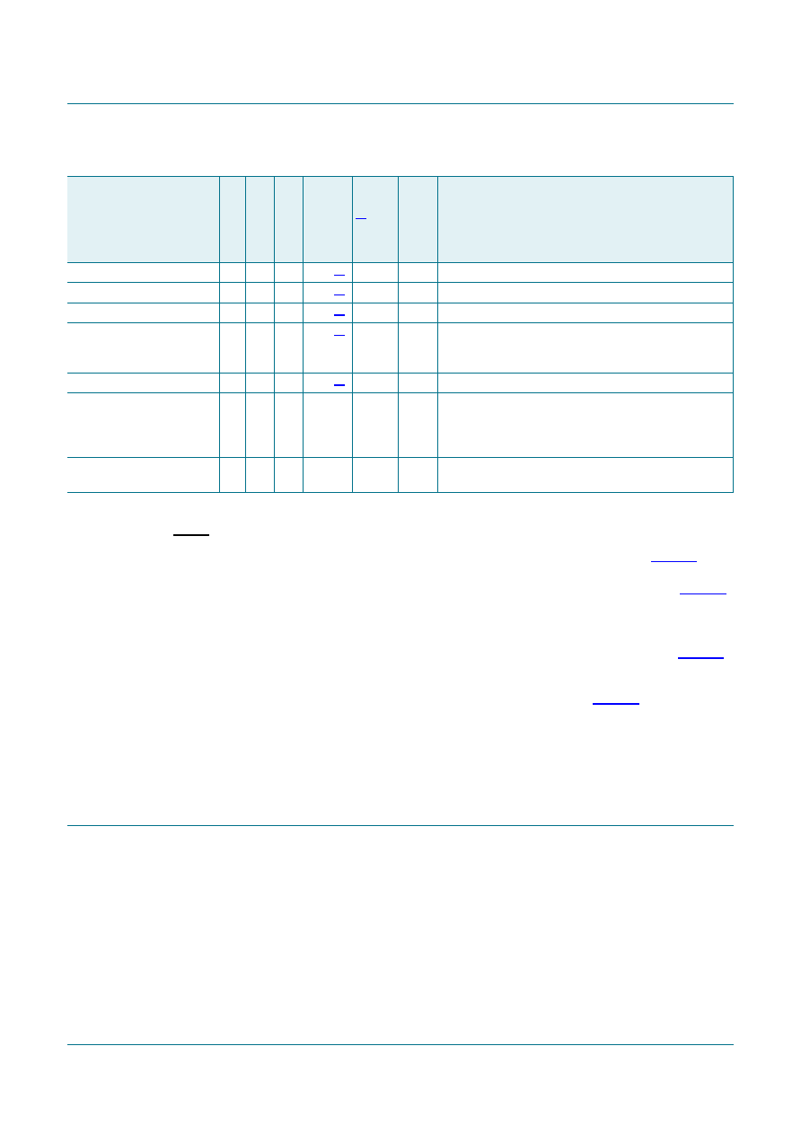
PIO1_31
-
25
-
I; PU
I/O
PIO1_31 — General purpose digital input/output pin.
USB_DM
13
G5
19
25
F-
USB_DM — USB bidirectional D
line.
USB_DP
14
H5
20
26
F-
USB_DP — USB bidirectional D+ line.
XTALIN
4
D1
6
8
-
Input to the oscillator circuit and internal clock
generator circuits. Input voltage must not exceed
1.8 V.
XTALOUT
5
E1
7
9
-
Output from the oscillator amplifier.
VDD
6;
29
B4;
E2
8;
44
10;
33;
48;
58
-
Supply voltage to the internal regulator, the external
rail, and the ADC. Also used as the ADC reference
voltage.
VSS
33
B5;
D2
5;
41
7;
54
-
Ground.
Table 3.
Pin description
Symbol
Pin
HVQFN33
Pi
n
TF
BGA
48
Pi
n
LQ
FP4
8
Pi
n
LQ
FP6
4
Reset
state
[1]
Type
Description
相关PDF资料 |
PDF描述 |
|---|---|
| 12RS153C | INDUCTOR RAD 15UH 4A T/H 10X10 |
| V375C12C75B2 | CONVERTER MOD DC/DC 12V 75W |
| GSM11DSEN-S243 | CONN EDGECARD 22POS .156 EYELET |
| LTC1558CS-3.3#TRPBF | IC BACKUP BATT CNTRLR3.3V 16SOIC |
| V375C12C75B | CONVERTER MOD DC/DC 12V 75W |
相关代理商/技术参数 |
参数描述 |
|---|---|
| OM13033 | 制造商:NXP Semiconductors 功能描述:EVAL ARM NGX LPC11U24 制造商:NXP Semiconductors 功能描述:LPC11U24, NGX, KEIL, EVAL BOARD 制造商:NXP Semiconductors 功能描述:LPC11U24, NGX, KEIL, EVAL BOARD; Silicon Manufacturer:NXP; Core Architecture:ARM; Core Sub-Architecture:Cortex-M0; Silicon Core Number:LPC11xxx; Silicon Family Name:LPC11Uxx; Features:Evaluation Board for LPC11U24 Microcontroller; ;RoHS Compliant: Yes |
| OM13033,598 | 功能描述:开发板和工具包 - ARM NGX LPC11U24 Eval Board RoHS:否 制造商:Arduino 产品:Development Boards 工具用于评估:ATSAM3X8EA-AU 核心:ARM Cortex M3 接口类型:DAC, ICSP, JTAG, UART, USB 工作电源电压:3.3 V |
| OM13033598 | 制造商:NXP Semiconductors 功能描述:EVAL ARM NGX LPC11U24 |
| OM13034,598 | 制造商:NXP Semiconductors 功能描述:EVAL, IAR, LPC1347, J-LINK LITE 制造商:NXP Semiconductors 功能描述:EVAL, IAR, LPC1347, J-LINK LITE, Silicon Manufacturer:NXP, Core Architecture:ARM 制造商:NXP Semiconductors 功能描述:EVAL, IAR, LPC1347, J-LINK LITE, Silicon Manufacturer:NXP, Core Architecture:ARM, Core Sub-Architecture:Cortex-M3, Silicon Core Number:LPC1347, Silicon Family Name:LPC1300, Kit Contents:Evaluation Board for LPC1347 , RoHS Compliant: Yes |
| OM13034598 | 制造商:NXP Semiconductors 功能描述:EVAL IAR LPC1347 J-LINK LITE |
发布紧急采购,3分钟左右您将得到回复。