- 您现在的位置:买卖IC网 > PDF目录299575 > OR3T306S240I-DB (LATTICE SEMICONDUCTOR CORP) FPGA, 196 CLBS, 48000 GATES, PQFP240 PDF资料下载
参数资料
| 型号: | OR3T306S240I-DB |
| 厂商: | LATTICE SEMICONDUCTOR CORP |
| 元件分类: | FPGA |
| 英文描述: | FPGA, 196 CLBS, 48000 GATES, PQFP240 |
| 封装: | PLASTIC, SQFP-240 |
| 文件页数: | 164/203页 |
| 文件大小: | 1368K |
| 代理商: | OR3T306S240I-DB |
第1页第2页第3页第4页第5页第6页第7页第8页第9页第10页第11页第12页第13页第14页第15页第16页第17页第18页第19页第20页第21页第22页第23页第24页第25页第26页第27页第28页第29页第30页第31页第32页第33页第34页第35页第36页第37页第38页第39页第40页第41页第42页第43页第44页第45页第46页第47页第48页第49页第50页第51页第52页第53页第54页第55页第56页第57页第58页第59页第60页第61页第62页第63页第64页第65页第66页第67页第68页第69页第70页第71页第72页第73页第74页第75页第76页第77页第78页第79页第80页第81页第82页第83页第84页第85页第86页第87页第88页第89页第90页第91页第92页第93页第94页第95页第96页第97页第98页第99页第100页第101页第102页第103页第104页第105页第106页第107页第108页第109页第110页第111页第112页第113页第114页第115页第116页第117页第118页第119页第120页第121页第122页第123页第124页第125页第126页第127页第128页第129页第130页第131页第132页第133页第134页第135页第136页第137页第138页第139页第140页第141页第142页第143页第144页第145页第146页第147页第148页第149页第150页第151页第152页第153页第154页第155页第156页第157页第158页第159页第160页第161页第162页第163页当前第164页第165页第166页第167页第168页第169页第170页第171页第172页第173页第174页第175页第176页第177页第178页第179页第180页第181页第182页第183页第184页第185页第186页第187页第188页第189页第190页第191页第192页第193页第194页第195页第196页第197页第198页第199页第200页第201页第202页第203页
Lattice Semiconductor
63
Data Sheet
November 2006
ORCA Series 3C and 3T FPGAs
Microprocessor Interface (MPI) (continued)
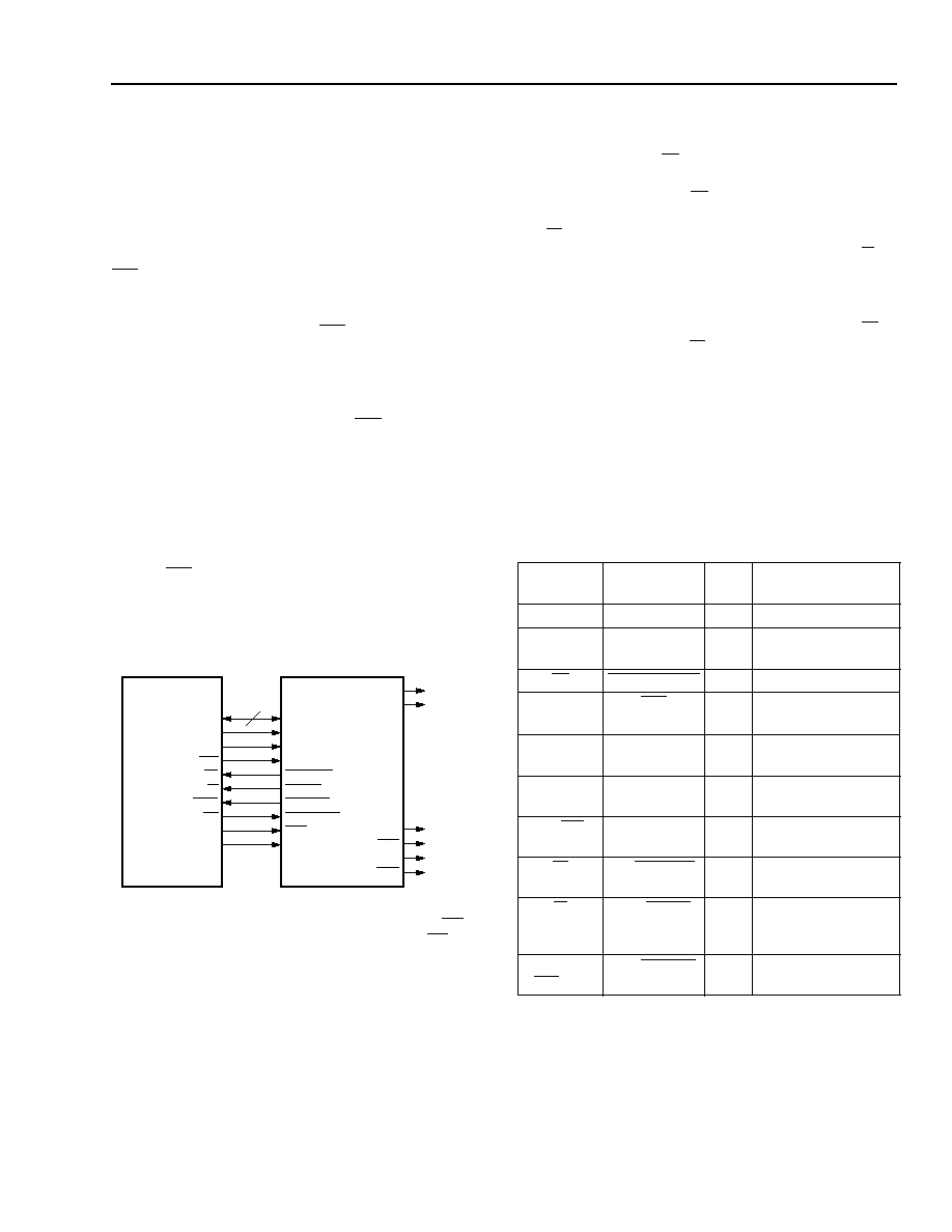
PowerPC System
In Figure 43, the
ORCA FPGA is a memory-mapped
peripheral to the
PowerPC processor. The PowerPC
interface uses separate address and data buses and
has several control lines. The
ORCA chip select lines,
CS0
and CS1, are each connected to an address line
coming from the
PowerPC. In this manner, the FPGA is
capable of a transaction with the
PowerPC whenever
the address line connected to CS0 is low, the address
line for CS1 is high, and there is a valid address on
PowerPC address lines A[27:31]. Other forms of selec-
tion are possible by using the FPGA chip selects in a
different way. For example,
PowerPC address bits
A[0:26] could be decoded to select CS0 and CS1, or if
the FPGA is the only peripheral to the
PowerPC, CS0
and CS1 could be tied low and high, respectively, to
cause them to always be selected. If the MPI is not
used for FPGA conguration, decoding logic can be
implemented internal or external to the FPGA. If logic
internal to the FPGA is used, the chip selects must be
routed out on an output pin and then connected exter-
nally to CS0 and/or CS1. If the MPI is to be used for
conguration, any decode logic used must be imple-
mented external to the FPGA since the FPGA logic has
not been congured yet.
5-5761(F)
Note: FPGA shown as a memory-mapped peripheral using CS0 and
CS1. Other decoding schemes are possible using CS0 and/or
CS1.
Figure 43.
PowerPC/MPI
The basic ow of a transaction on the
PowerPC/MPI
interface is given below. Pin descriptions are shown in
Table 16 and timing is shown in the Timing Characteris-
tics section of this data sheet. For both read and write
transactions, the address, chip select, and read/write
(read high, write low) signals are set up at the FPGA
pins by the
PowerPC. The PowerPC then asserts its
transfer start signal (TS) low. Data is available to the
MPI
during a write at the rising clock edge after the
clock cycle during which TS is low. The transfer is
acknowledged to the
PowerPC by the low asser tion of
the TA signal. The MPI
PowerPC interface does not
support burst transfers, so the burst inhibit signal, BI, is
also asserted low during the transfer acknowledge . The
same process applies to a read from the MPI except
that the read data is expected at the FPGA data pins by
the
PowerPC at the rising edge of the clock when TA is
low. The MPI only drives TA low for one clock cycle.
Interrupt requests can be sent to the
PowerPC asyn-
chronously to the read/write process. Interrupt requests
are sourced by the user-logic in the FPGA. The MPI will
assert the request to the
PowerPC as a direct interrupt
signal and/or a pollable bit in the MPI status register
(discussed in the MPI Setup and Control section). The
MPI
will continue to assert the interrupt request until
the user-logic deasserts its interrupt request signal.
Table 16.
PowerPC/MPI Conguration
DOUT
CCLK
D[7:0]
A[4:0]
MPI_CLK
MPI_RW
MPI_ACK
MPI_BI
MPI_IRQ
MPI_STRB
CS0
CS1
HDC
LDC
D[7:0]
A[27:31]
CLKOUT
RD/WR
TA
BI
IRQx
TS
A26
A25
TO DAISY-
CHAINED
DEVICES
POWERPC
ORCA
8
FPGA
SERIES 3
DONE
INIT
PowerPC
Signal
ORCA Pin
Name
MPI
I/O
Function
D[0:7]
D[7:0]
I/O
8-bit data bus
A[27:31]
A[4:0]
I
5-bit
MPI address
bus
TS
RD/MPI_STRB
I
Transfer start signal
—
CS0
I
Active-low
MPI
select
—
CS1
I
Active-high
MPI
select
CLKOUT
A7/MPI_CLK
I
PowerPC interface
clock
RD/WR
A8/MPI_RW
I
Read (high)/write
(low) signal
TA
A9/MPI_ACK
O
Active-low transfer
acknowledge signal
BI
A10/MPI_BI
O
Active-low burst
transfer inhibit
signal
Any of
IRQ
[7:0]
A11/MPI_IRQ
O
Active-low interrupt
request signal
Select
devices
have
been
discontinued.
See
Ordering
Information
section
for
product
status.
相关PDF资料 |
PDF描述 |
|---|---|
| OR3T307S240-DB | FPGA, 196 CLBS, 48000 GATES, PQFP240 |
| OR3T556PS240-DB | FPGA, 324 CLBS, 80000 GATES, PQFP240 |
| OR3T806PS240-DB | FPGA, 484 CLBS, 116000 GATES, PQFP240 |
| OR3T807PS240-DB | FPGA, 484 CLBS, 116000 GATES, PQFP240 |
| OR3T55-4BA256I | FPGA, 324 CLBS, 40000 GATES, 80 MHz, PBGA256 |
相关代理商/技术参数 |
参数描述 |
|---|---|
| OR3T30-7BA256 | 制造商:AGERE 制造商全称:AGERE 功能描述:3C and 3T Field-Programmable Gate Arrays |
| OR3T307BA256-DB | 功能描述:FPGA - 现场可编程门阵列 1568 LUT 221 I/O RoHS:否 制造商:Altera Corporation 系列:Cyclone V E 栅极数量: 逻辑块数量:943 内嵌式块RAM - EBR:1956 kbit 输入/输出端数量:128 最大工作频率:800 MHz 工作电源电压:1.1 V 最大工作温度:+ 70 C 安装风格:SMD/SMT 封装 / 箱体:FBGA-256 |
| OR3T30-7BA256I | 制造商:AGERE 制造商全称:AGERE 功能描述:3C and 3T Field-Programmable Gate Arrays |
| OR3T30-7BA352 | 制造商:AGERE 制造商全称:AGERE 功能描述:3C and 3T Field-Programmable Gate Arrays |
| OR3T30-7BA352I | 制造商:AGERE 制造商全称:AGERE 功能描述:3C and 3T Field-Programmable Gate Arrays |
发布紧急采购,3分钟左右您将得到回复。