- 您现在的位置:买卖IC网 > PDF目录299575 > OR3T306S240I-DB (LATTICE SEMICONDUCTOR CORP) FPGA, 196 CLBS, 48000 GATES, PQFP240 PDF资料下载
参数资料
| 型号: | OR3T306S240I-DB |
| 厂商: | LATTICE SEMICONDUCTOR CORP |
| 元件分类: | FPGA |
| 英文描述: | FPGA, 196 CLBS, 48000 GATES, PQFP240 |
| 封装: | PLASTIC, SQFP-240 |
| 文件页数: | 17/203页 |
| 文件大小: | 1368K |
| 代理商: | OR3T306S240I-DB |
第1页第2页第3页第4页第5页第6页第7页第8页第9页第10页第11页第12页第13页第14页第15页第16页当前第17页第18页第19页第20页第21页第22页第23页第24页第25页第26页第27页第28页第29页第30页第31页第32页第33页第34页第35页第36页第37页第38页第39页第40页第41页第42页第43页第44页第45页第46页第47页第48页第49页第50页第51页第52页第53页第54页第55页第56页第57页第58页第59页第60页第61页第62页第63页第64页第65页第66页第67页第68页第69页第70页第71页第72页第73页第74页第75页第76页第77页第78页第79页第80页第81页第82页第83页第84页第85页第86页第87页第88页第89页第90页第91页第92页第93页第94页第95页第96页第97页第98页第99页第100页第101页第102页第103页第104页第105页第106页第107页第108页第109页第110页第111页第112页第113页第114页第115页第116页第117页第118页第119页第120页第121页第122页第123页第124页第125页第126页第127页第128页第129页第130页第131页第132页第133页第134页第135页第136页第137页第138页第139页第140页第141页第142页第143页第144页第145页第146页第147页第148页第149页第150页第151页第152页第153页第154页第155页第156页第157页第158页第159页第160页第161页第162页第163页第164页第165页第166页第167页第168页第169页第170页第171页第172页第173页第174页第175页第176页第177页第178页第179页第180页第181页第182页第183页第184页第185页第186页第187页第188页第189页第190页第191页第192页第193页第194页第195页第196页第197页第198页第199页第200页第201页第202页第203页
Lattice Semiconductor
113
Data Sheet
November 2006
ORCA Series 3C and 3T FPGAs
Timing Characteristics (continued)
Special Function Blocks Timing
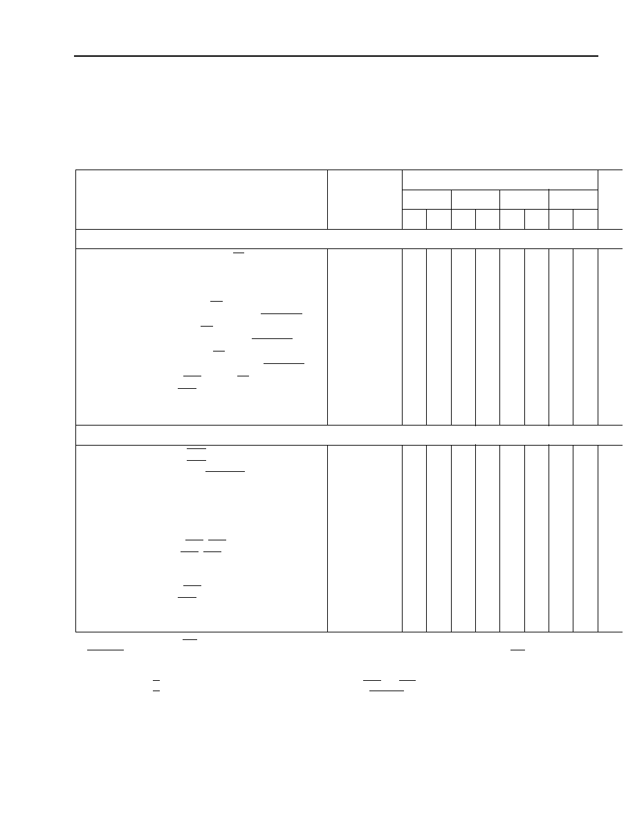
Table 49. Microprocessor Interface (MP I)Timing Characteristics
OR3Cxx Commercial: VDD = 5.0 V ± 5%, 0 °C
< TA < 70 °C; Industrial: VDD = 5.0 V ± 10%, –40 °C < TA < +85 °C.
OR3Txxx Commercial: VDD = 3.0 V to 3.6 V, 0 °C
< TA < 70 °C; Industrial: VDD = 3.0 V to 3.6 V, –40 °C < TA < +85 °C.
1. For user system exibility, CS0 and CS1 may be set up to any one of the three rising clock edges, beginning with the rising clock edge when
MPI_STRB
is low. If both chip selects are valid and the setup time is met, the MPI will latch the chip select state, and CS0 and CS1 may go
inactive before the end of the read/write cycle.
2. 0.5 MPI_CLK.
3. Write data and W/R have to be valid starting from the clock cycle after both ADS and CS0 and CS1 are recognized.
4. Write data and W/R have to be held until the microprocessor receives a valid RDYRCV.
Notes:
Read and write descriptions are referenced to the host microprocessor; e.g., a read is a read by the host (
PowerPC, i960) from the FPGA.
PowerPC and i960 timings to/from the clock are relative to the clock at the FPGA microprocessor interface clock pin (MPI_CLK).
Parameter
Symbol
Speed
Unit
–4
–5
–6
–7
Min Max Min Max Min Max Min Max
PowerPC Interface Timing
(TJ = 85 °C, VDD = min)
Transfer Acknowledge Delay (CLK to TA)
Burst Inhibit Delay (CLK to BIN)
Transfer Acknowledge Delay to High Impedance
Burst Inhibit Delay to High Impedance
Write Data Setup Time (data to TS)
Write Data Hold Time (data from CLK while MPI_ACK low)
Address Setup Time (addr to TS)
Address Hold Time (addr from CLK while MPI_ACK low)
Read/Write Setup Time (R/W to TS)
Read/Write Hold Time (R/W from CLK while MPI_ACK low)
Chip Select Setup Time (CS0, CS1 to TS)
Chip Select Hold Time (CS0, CS1 from CLK)
User Address Delay (pad to UA[3:0])
User Read/Write Delay (pad to URDWR_DEL)
TA_DEL
BI_DEL
TA_DELZ
BI_DELZ
WD_SET
WD_HLD
A_SET
A_HLD
RW_SET
RW_HLD
CS_SET
CS_HLD
UA_DEL
URDWR_DEL
—
0.0
0.3
0.0
—
11.6
(2)
—
3.3
7.0
—
0.0
.25
0.0
—
9.3
(2)
—
2.6
5.4
—
0.0
.14
0.0
—
8.0
(2)
—
2.3
4.2
—
0.0
.12
0.0
—
6.8
(2)
—
1.9
3.6
ns
i960 Interface Timing
(TJ = 85 °C, VDD = min)
Addr/Data Select to ALE (ADS, to ALE low)
Addr/Data Select to ALE (ADS, from ALE low)
Ready/Receive Delay (CLK to RDYRCV)
Ready/Receive Delay to High Impedance
Write Data Setup Time
Write Data Hold Time
Address Setup Time (addr to ALE low)
Address Hold Time (addr from ALE low)
Byte Enable Setup Time (BE0, BE1 to ALE low)
Byte Enable Hold Time (BE0, BE1 from ALE low)
Read/Write Setup Time
Read/Write Hold Time
Chip Select Setup Time (CS0, CS1 to CLK)(1)
Chip Select Hold Time (CS0, CS1 from CLK)(1)
User Address Delay (CLK low to UA[3:0])
User Read/Write Delay (pad to URDWR_DEL)
ADSN_SET
ADSN_HLD
RDYRCV_DEL
RDYRCV_DELZ
WD_SET
WD_HLD
A_SET
A_HLD
BE_SET
BE_HLD
RW_SET
RW_HLD
CS_SET
CS_HLD
UA_DEL
URDWR_DEL
2.0
0.0
—
(3)
(4)
2.0
(3)
(4)
2.0
0.0
—
11.6
(2)
—
6.6
7.0
1.8
0.0
—
(3)
(4)
1.8
(3)
(4)
1.8
0.0
—
9.3
(2)
—
4.3
5.4
1.6
0.0
—
(3)
(4)
0.50
0.51
0.50
0.51
(3)
(4)
0.45
0.0
—
8.0
(2)
—
4.1
4.2
1.4
0.0
—
(3)
(4)
—
(3)
(4)
—
0.0
—
6.8
(2)
—
0.42
0.44
0.42
0.44
—
0.38
—
3.5
3.6
ns
Select
devices
have
been
discontinued.
See
Ordering
Information
section
for
product
status.
相关PDF资料 |
PDF描述 |
|---|---|
| OR3T307S240-DB | FPGA, 196 CLBS, 48000 GATES, PQFP240 |
| OR3T556PS240-DB | FPGA, 324 CLBS, 80000 GATES, PQFP240 |
| OR3T806PS240-DB | FPGA, 484 CLBS, 116000 GATES, PQFP240 |
| OR3T807PS240-DB | FPGA, 484 CLBS, 116000 GATES, PQFP240 |
| OR3T55-4BA256I | FPGA, 324 CLBS, 40000 GATES, 80 MHz, PBGA256 |
相关代理商/技术参数 |
参数描述 |
|---|---|
| OR3T30-7BA256 | 制造商:AGERE 制造商全称:AGERE 功能描述:3C and 3T Field-Programmable Gate Arrays |
| OR3T307BA256-DB | 功能描述:FPGA - 现场可编程门阵列 1568 LUT 221 I/O RoHS:否 制造商:Altera Corporation 系列:Cyclone V E 栅极数量: 逻辑块数量:943 内嵌式块RAM - EBR:1956 kbit 输入/输出端数量:128 最大工作频率:800 MHz 工作电源电压:1.1 V 最大工作温度:+ 70 C 安装风格:SMD/SMT 封装 / 箱体:FBGA-256 |
| OR3T30-7BA256I | 制造商:AGERE 制造商全称:AGERE 功能描述:3C and 3T Field-Programmable Gate Arrays |
| OR3T30-7BA352 | 制造商:AGERE 制造商全称:AGERE 功能描述:3C and 3T Field-Programmable Gate Arrays |
| OR3T30-7BA352I | 制造商:AGERE 制造商全称:AGERE 功能描述:3C and 3T Field-Programmable Gate Arrays |
发布紧急采购,3分钟左右您将得到回复。