- 您现在的位置:买卖IC网 > PDF目录299576 > OR3T55-4BA256 FPGA, 324 CLBS, 40000 GATES, 80 MHz, PBGA256 PDF资料下载
参数资料
| 型号: | OR3T55-4BA256 |
| 元件分类: | FPGA |
| 英文描述: | FPGA, 324 CLBS, 40000 GATES, 80 MHz, PBGA256 |
| 封装: | PLASTIC, BGA-256 |
| 文件页数: | 35/210页 |
| 文件大小: | 2138K |
| 代理商: | OR3T55-4BA256 |
第1页第2页第3页第4页第5页第6页第7页第8页第9页第10页第11页第12页第13页第14页第15页第16页第17页第18页第19页第20页第21页第22页第23页第24页第25页第26页第27页第28页第29页第30页第31页第32页第33页第34页当前第35页第36页第37页第38页第39页第40页第41页第42页第43页第44页第45页第46页第47页第48页第49页第50页第51页第52页第53页第54页第55页第56页第57页第58页第59页第60页第61页第62页第63页第64页第65页第66页第67页第68页第69页第70页第71页第72页第73页第74页第75页第76页第77页第78页第79页第80页第81页第82页第83页第84页第85页第86页第87页第88页第89页第90页第91页第92页第93页第94页第95页第96页第97页第98页第99页第100页第101页第102页第103页第104页第105页第106页第107页第108页第109页第110页第111页第112页第113页第114页第115页第116页第117页第118页第119页第120页第121页第122页第123页第124页第125页第126页第127页第128页第129页第130页第131页第132页第133页第134页第135页第136页第137页第138页第139页第140页第141页第142页第143页第144页第145页第146页第147页第148页第149页第150页第151页第152页第153页第154页第155页第156页第157页第158页第159页第160页第161页第162页第163页第164页第165页第166页第167页第168页第169页第170页第171页第172页第173页第174页第175页第176页第177页第178页第179页第180页第181页第182页第183页第184页第185页第186页第187页第188页第189页第190页第191页第192页第193页第194页第195页第196页第197页第198页第199页第200页第201页第202页第203页第204页第205页第206页第207页第208页第209页第210页
Lucent Technologies Inc.
13
Preliminary Data Sheet, Rev. 1
September 1998
ORCA Series 3 FPGAs
Programmable Logic Cells (continued)
Half-Logic Mode
Series 3 of FPGAs is based upon a twin-quad architec-
ture in the PFUs. The byte-wide nature (eight LUTs,
eight latches/FFs) may just as easily be viewed as two
nibbles (two sets of four LUTs, four latches/FFs). The
two nibbles of the PFU are organized so that any nib-
ble-wide feature (excluding some softwired LUT topolo-
gies) can be swapped with any other nibble-wide
feature in another PFU. This provides for very flexible
use of logic and for extremely flexible routing. The half-
logic mode of the PFU takes advantage of the twin-
quad architecture and allows half of a PFU, K[7:4] and
associated latches/FFs, to be used in logic mode while
the other half of the PFU, K[3:0] and associated latches/
FFs, is used in ripple mode. In half-logic mode, the
ninth FF may be used as a general-purpose FF or as a
register in the ripple mode carry chain.
Ripple Mode
The PFU LUTs can be combined to do byte-wide ripple
functions with high-speed carry logic. Each LUT has a
dedicated carry-out net to route the carry to/from any
adjacent LUT. Using the internal carry circuits, fast
arithmetic, counter, and comparison functions can be
implemented in one PFU. Similarly, each PFU has
carry-in (CIN, FCIN) and carry-out (COUT, FCOUT)
ports for fast-carry routing between adjacent PFUs.
The ripple mode is generally used in operations on two
data buses. A single PFU can support an 8-bit ripple
function. Data buses of 4 bits and less can use the
nibble-wide ripple chain that is available in half-logic
mode. This nibble-wide ripple chain is also useful for
longer ripple chains where the length modulo 8 is four
or less. For example, a 12-bit adder (12 modulo 8 = 4)
can be implemented in one PFU in ripple mode (8 bits)
and one PFU in half-logic mode (4 bits), freeing half of
a PFU for general logic mode functions.
Each LUT has two operands and a ripple (generally
carry) input, and provides a result and ripple (generally
carry) output. A single bit is rippled from the previous
LUT and is used as input into the current LUT. For LUT
K0, the ripple input is from the PFU CIN or FCIN port.
The CIN/FCIN data can come from either the fast-carry
routing (FCIN) or the PFU input (CIN), or it can be tied
to logic 1 or logic 0.
In the following discussions, the notations LUT K7/K3
and F[7:0]/F[3:0] are used to denote the LUT that pro-
vides the carry-out and the data outputs for full PFU
ripple operation (K7, F[7:0]) and half-logic ripple
operation (K3, F[3:0]), respectively. The ripple mode
diagram in Figure 6 shows full PFU ripple operation,
with half-logic ripple connections shown as dashed
lines.
The result output and ripple output are calculated by
using generate/propagate circuitry. In ripple mode, the
two operands are input into KZ[1] and KZ[0] of each
LUT. The result bits, one per LUT, are F[7:0]/F[3:0] (see
Figure 6). The ripple output from LUT K7/K3 can be
routed on dedicated carry circuitry into any of four adja-
cent PLCs, and it can be placed on the PFU COUT/
FCOUT outputs. This allows the PLCs to be cascaded
in the ripple mode so that nibble-wide ripple functions
can be expanded easily to any length.
Result outputs and the carry-out may optionally be reg-
istered within the PFU. The capability to register the
ripple results, including the carry output, provides for
improved counter performance and simplified pipelin-
ing in arithmetic functions.
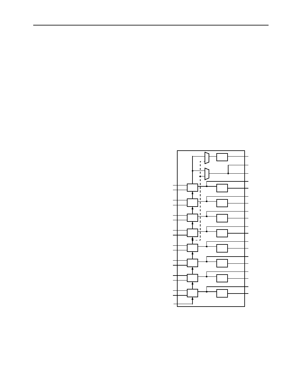
Figure 6. Ripple Mode
5-5755(F)
F7
K7[1]
K7[0]
K7
D
Q
C
DQ
Q7
REGCOUT
COUT
F6
K6[1]
K6[0]
K6
D
Q
Q6
F4
K4[1]
K4[0]
K4
D
Q
Q4
F3
K3[1]
K3[0]
K3
D
Q
Q3
F2
K2[1]
K2[0]
K2
D
Q
Q2
F1
K1[1]
K1[0]
K1
D
Q
Q1
F5
K5[1]
K5[0]
K5
D
Q
Q5
F0
K0[1]
K0[0]
K0
D
Q
Q0
CIN/FCIN
FCOUT
相关PDF资料 |
PDF描述 |
|---|---|
| OR3T55-4BA352I | FPGA, 324 CLBS, 40000 GATES, 80 MHz, PBGA352 |
| OR3T55-4BA352 | FPGA, 324 CLBS, 40000 GATES, 80 MHz, PBGA352 |
| OR3T80-4BA352I | FPGA, 484 CLBS, 58000 GATES, 80 MHz, PBGA352 |
| OR3T80-4BA352 | FPGA, 484 CLBS, 58000 GATES, 80 MHz, PBGA352 |
| OR3T125-4BC432I | FPGA, 784 CLBS, 92000 GATES, 80 MHz, PBGA432 |
相关代理商/技术参数 |
参数描述 |
|---|---|
| OR3T55-4BA256I | 制造商:未知厂家 制造商全称:未知厂家 功能描述:Field Programmable Gate Array (FPGA) |
| OR3T55-4PS208I | 制造商:未知厂家 制造商全称:未知厂家 功能描述:Field Programmable Gate Array (FPGA) |
| OR3T55-4PS240I | 制造商:未知厂家 制造商全称:未知厂家 功能描述:Field Programmable Gate Array (FPGA) |
| OR3T55-5BA256 | 制造商:AGERE 制造商全称:AGERE 功能描述:3C and 3T Field-Programmable Gate Arrays |
| OR3T55-5BA256I | 制造商:AGERE 制造商全称:AGERE 功能描述:3C and 3T Field-Programmable Gate Arrays |
发布紧急采购,3分钟左右您将得到回复。