- 您现在的位置:买卖IC网 > PDF目录15542 > P0037 (Terasic Technologies Inc)BOARD DEV/EDUCATION ALTERA DE0 PDF资料下载
参数资料
| 型号: | P0037 |
| 厂商: | Terasic Technologies Inc |
| 文件页数: | 26/34页 |
| 文件大小: | 0K |
| 描述: | BOARD DEV/EDUCATION ALTERA DE0 |
| 产品培训模块: | Cyclone® III FPGA |
| 标准包装: | 1 |
| 类型: | FPGA |
| 适用于相关产品: | Cyclone III |
| 所含物品: | 板,线缆,CD,电源 |
| 相关产品: | 544-2541-ND - IC CYCLONE III FPGA 16K 164 MBGA 544-2540-ND - IC CYCLONE III FPGA 16K 144 EQFP 544-2480-ND - IC CYCLONE III FPGA 16K 484UBGA 544-2478-ND - IC CYCLONE III FPGA 16K 484UBGA 544-2477-ND - IC CYCLONE III FPGA 16K 484UBGA 544-2476-ND - IC CYCLONE III FPGA 16K 484UBGA 544-2474-ND - IC CYCLONE III FPGA 16K 484FBGA 544-2473-ND - IC CYCLONE III FPGA 16K 484FBGA 544-2472-ND - IC CYCLONE III FPGA 16K 484FBGA 544-2471-ND - IC CYCLONE III FPGA 16K 484FBGA 更多... |
第1页第2页第3页第4页第5页第6页第7页第8页第9页第10页第11页第12页第13页第14页第15页第16页第17页第18页第19页第20页第21页第22页第23页第24页第25页当前第26页第27页第28页第29页第30页第31页第32页第33页第34页
�� �
�
�1–26�
�Chapter� 1:� Cyclone� III� Device� Datasheet�
�I/O� Timing�
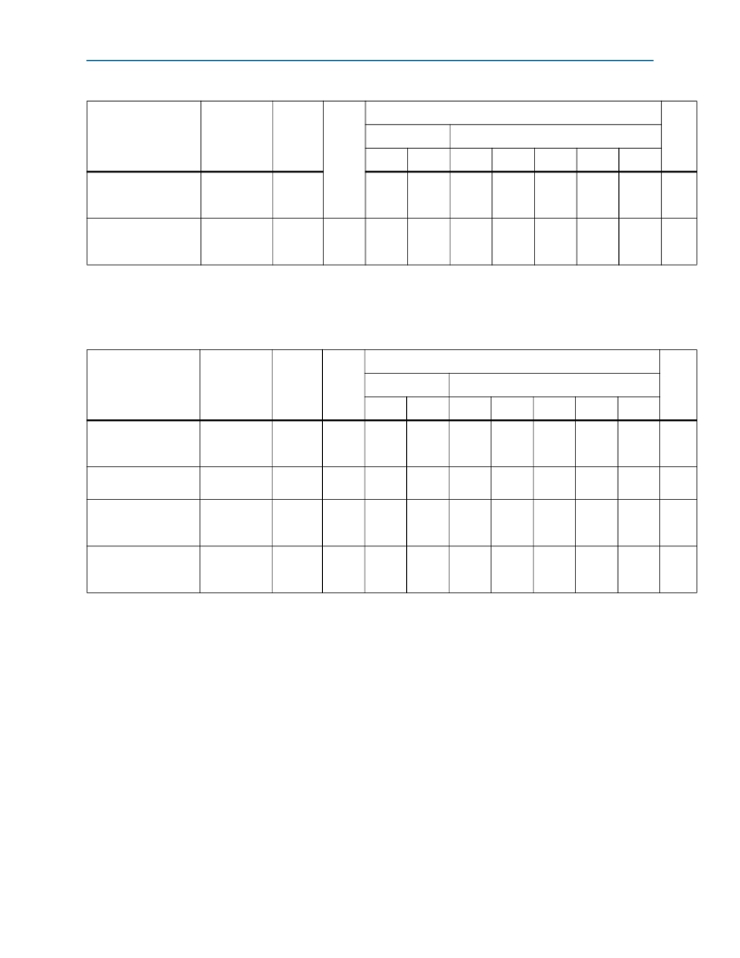
�Table� 1–37.� Cyclone� III� Devices� IOE� Programmable� Delay� on� Column� Pins� (1)� ,�
�(2)�
�(Part� 2� of� 2)�
�Max� Offset�
�Parameter�
�Paths�
�Affected�
�Number�
�of�
�Settings�
�Min�
�Offset�
�Fast� Corner�
�Slow� Corner�
�Unit�
�A7,� I7�
�C6�
�C6�
�C7�
�C8�
�I7�
�A7�
�Delay� from� output�
�register� to� output� pin�
�I/O� output�
�register� to�
�pad�
�2�
�0�
�0.479�
�0.504�
�0.915�
�1.011�
�1.107�
�1.018�
�1.048�
�ns�
�Input� delay� from�
�Pad� to� global�
�dual-purpose� clock� pin�
�clock�
�12�
�0�
�0.664�
�0.694�
�1.199�
�1.378�
�1.532�
�1.392�
�1.441�
�ns�
�to� fan-out� destinations�
�network�
��(1)� The� incremental� values� for� the� settings� are� generally� linear.� For� exact� values� of� each� setting,� use� the� latest� version� of� the� Quartus� II� software.�
�(2)� The� minimum� and� maximum� offset� timing� numbers� are� in� reference� to� setting� ‘0’� as� available� in� the� Quartus� II� software.�
�Table� 1–38.� Cyclone� III� Devices� IOE� Programmable� Delay� on� Row� Pins�
��Max� Offset�
�Parameter�
�Paths�
�Affected�
�Number�
�of�
�Settings�
�Min�
�Offset�
�Fast� Corner�
�Slow� Corner�
�Unit�
�A7,� I7�
�C6�
�C6�
�C7�
�C8�
�I7�
�A7�
�Input� delay� from� pin� to�
�internal� cells�
�Input� delay� from� pin� to�
�input� register�
�Delay� from� output�
�register� to� output� pin�
�Input� delay� from�
�dual-purpose� clock� pin�
�to� fan-out� destinations�
�Pad� to� I/O�
�dataout� to�
�core�
�Pad� to� I/O�
�input� register�
�I/O� output�
�register� to�
�pad�
�Pad� to� global�
�clock� network�
�7�
�8�
�2�
�12�
�0�
�0�
�0�
�0�
�1.209�
�1.207�
�0.51�
�0.669�
�1.314�
�1.312�
�0.537�
�0.698�
�2.174�
�2.202�
�0.962�
�1.207�
�2.335�
�2.402�
�1.072�
�1.388�
�2.406�
�2.558�
�1.167�
�1.542�
�2.381�
�2.447�
�1.074�
�1.403�
�2.505�
�2.557�
�1.101�
�1.45�
�ns�
�ns�
�ns�
�ns�
��(1)� The� incremental� values� for� the� settings� are� generally� linear.� For� exact� values� of� each� setting,� use� the� latest� version� of� Quartus� II� software.�
�(2)� The� minimum� and� maximum� offset� timing� numbers� are� in� reference� to� setting� ‘0’� as� available� in� the� Quartus� II� software�
�I/O� Timing�
�You� can� use� the� following� methods� to� determine� the� I/O� timing:�
�■�
�■�
�the� Excel-based� I/O� Timing.�
�the� Quartus� II� timing� analyzer.�
�The� Excel-based� I/O� Timing� provides� pin� timing� performance� for� each� device� density�
�and� speed� grade.� The� data� is� typically� used� prior� to� designing� the� FPGA� to� get� a�
�timing� budget� estimation� as� part� of� the� link� timing� analysis.� The� Quartus� II� timing�
�analyzer� provides� a� more� accurate� and� precise� I/O� timing� data� based� on� the� specifics�
�of� the� design� after� place-and-route� is� complete.�
���July� 2012� Altera� Corporation�
�相关PDF资料 |
PDF描述 |
|---|---|
| MAX16023PTAT12+T | IC BATTERY BACKUP 1.2V 8TDFN-EP |
| TWR-MCF51CN-KIT | KIT TOWER BOARD/SERIAL/ELEVATOR |
| MAX16023PTAS25+T | IC BATTERY BACKUP 2.5V 8TDFN-EP |
| MAX16023PTAS18+T | IC BATTERY BACKUP 1.8V 8TDFN-EP |
| MAX16023PTAS12+T | IC BATTERY BACKUP 1.2V 8TDFN-EP |
相关代理商/技术参数 |
参数描述 |
|---|---|
| P0037 (ACADEMIC) | 制造商:Terasic 功能描述:(DE0) 3C16 - ACADEMIC PRICE |
| P0038 | 功能描述:子卡和OEM板 ETHERNET - HSMC CARD (HSMC-NET) RoHS:否 制造商:BeagleBoard by CircuitCo 产品:BeagleBone LCD4 Boards 用于:BeagleBone - BB-Bone - Open Source Development Kit |
| P0039 | 功能描述:子卡和OEM板 SDI - HSMC CARD (SDI-HSMC) RoHS:否 制造商:BeagleBoard by CircuitCo 产品:BeagleBone LCD4 Boards 用于:BeagleBone - BB-Bone - Open Source Development Kit |
| P003KDKB | 制造商:Hammond Power Solutions 功能描述:POTTED 3PH N3R CU CLASS 1, DIV II 3kVA 480-240 |
| P0040 | 功能描述:子卡和OEM板 SFP - HSMC CARD (SFP-HSMC) RoHS:否 制造商:BeagleBoard by CircuitCo 产品:BeagleBone LCD4 Boards 用于:BeagleBone - BB-Bone - Open Source Development Kit |
发布紧急采购,3分钟左右您将得到回复。