- 您现在的位置:买卖IC网 > PDF目录12010 > P89V52X2FBD,157 (NXP Semiconductors)IC 80C51 MCU FLASH 8K 44-LQFP PDF资料下载
参数资料
| 型号: | P89V52X2FBD,157 |
| 厂商: | NXP Semiconductors |
| 文件页数: | 55/57页 |
| 文件大小: | 0K |
| 描述: | IC 80C51 MCU FLASH 8K 44-LQFP |
| 产品培训模块: | Migrating from 8/16-Bit MCUs to 32-Bit ARMs |
| 标准包装: | 800 |
| 系列: | 89V |
| 核心处理器: | 8051 |
| 芯体尺寸: | 8-位 |
| 速度: | 40MHz |
| 连通性: | UART/USART |
| 外围设备: | POR |
| 输入/输出数: | 32 |
| 程序存储器容量: | 8KB(8K x 8) |
| 程序存储器类型: | 闪存 |
| EEPROM 大小: | 192 x 8 |
| RAM 容量: | 256 x 8 |
| 电压 - 电源 (Vcc/Vdd): | 2.7 V ~ 5.5 V |
| 振荡器型: | 外部 |
| 工作温度: | -40°C ~ 85°C |
| 封装/外壳: | 44-LQFP |
| 包装: | 托盘 |
| 配用: | 622-1017-ND - BOARD 44-ZIF PLCC SOCKET 622-1012-ND - BOARD FOR P89V52X2 44-TQFP 622-1008-ND - BOARD FOR LPC9103 10-HVSON |
| 其它名称: | 568-4250 935282529157 P89V52X2FBD |
第1页第2页第3页第4页第5页第6页第7页第8页第9页第10页第11页第12页第13页第14页第15页第16页第17页第18页第19页第20页第21页第22页第23页第24页第25页第26页第27页第28页第29页第30页第31页第32页第33页第34页第35页第36页第37页第38页第39页第40页第41页第42页第43页第44页第45页第46页第47页第48页第49页第50页第51页第52页第53页第54页当前第55页第56页第57页
P89V52X2_3
NXP B.V. 2009. All rights reserved.
Product data sheet
Rev. 03 — 4 May 2009
7 of 57
NXP Semiconductors
P89V52X2
80C51 with 256 B RAM, 192 B data EEPROM
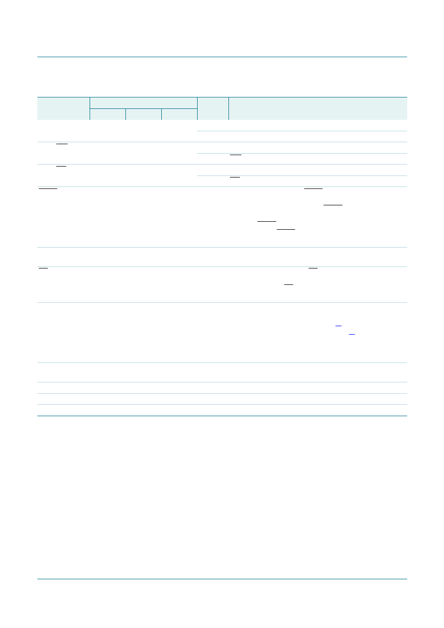
[1]
ALE loading issue: When ALE pin experiences higher loading (> 30 pF) during the reset, the microcontroller may accidentally enter into
modes other than normal working mode. The solution is to add a pull-up resistor of 3 k
to 50 k to V
DD, e.g., for ALE pin.
[2]
For 6-clock mode, ALE is emitted at 1
3 of crystal frequency.
P3[5]/T1
15
11
17
I/O
P3[5] — Port 3 bit 5.
I
T1 — External count input to Timer/Counter 1
P3[6]/WR
16
12
18
O
P3[6] — Port 3 bit 6.
O
WR — External data memory write strobe
P3[7]/RD
17
13
19
O
P3[7] — Port 3 bit 7.
O
RD — External data memory read strobe.
PSEN
29
26
32
I/O
Program Store Enable: PSEN is the read strobe for
external program memory. When the device is executing
from internal program memory, PSEN is inactive (HIGH).
When the device is executing code from external program
memory, PSEN is activated twice each machine cycle,
except that two PSEN activations are skipped during each
access to external data memory.
RST
9
4
10
I
Reset: While the oscillator is running, a HIGH logic state
on this pin for two machine cycles will reset the device.
EA
31
29
35
I
External Access Enable: EA must be connected to VSS in
order to enable the device to fetch code from the external
program memory. EA must be strapped to VDD for internal
program execution.
ALE
30
27
33
I/O
Address Latch Enable: ALE is the output signal for
latching the low byte of the address during an access to
external memory. Normally the ALE[1] is emitted at a
constant rate of 1
6 the crystal frequency[2] and can be
used for external timing and clocking. One ALE pulse is
skipped during each access to external data memory.
However, if AO is set to ‘1’, ALE is disabled.
XTAL1
19
15
21
I
Crystal 1: Input to the inverting oscillator amplier and
input to the internal clock generator circuits.
XTAL2
18
14
20
O
Crystal 2: Output from the inverting oscillator amplier.
VDD
40
38
44
I
Power supply
VSS
20
16
22
I
Ground
Table 2.
Pin description …continued
Symbol
Pin
Type
Description
DIP40
LQFP44
PLCC44
相关PDF资料 |
PDF描述 |
|---|---|
| P89V52X2FA,512 | IC 80C51 MCU FLASH 8K 44-PLCC |
| VJ2225Y104KBLAT4X | CAP CER 0.1UF 630V 10% X7R 2225 |
| LPC2292FET144/G,55 | IC ARM7 MCU FLASH 256K 144TFBGA |
| VI-JWM-IY-F4 | CONVERTER MOD DC/DC 10V 50W |
| VI-JWL-IY-F3 | CONVERTER MOD DC/DC 28V 50W |
相关代理商/技术参数 |
参数描述 |
|---|---|
| P89V52X2FN | 制造商:PHILIPS 制造商全称:NXP Semiconductors 功能描述:8-bit 80C51 low power 8 kB flash microcontroller with 256 B RAM, 192 B data EEPROM |
| P89V52X2FN,112 | 功能描述:8位微控制器 -MCU 80C51 8K FL / 256 RM RoHS:否 制造商:Silicon Labs 核心:8051 处理器系列:C8051F39x 数据总线宽度:8 bit 最大时钟频率:50 MHz 程序存储器大小:16 KB 数据 RAM 大小:1 KB 片上 ADC:Yes 工作电源电压:1.8 V to 3.6 V 工作温度范围:- 40 C to + 105 C 封装 / 箱体:QFN-20 安装风格:SMD/SMT |
| P89V660 | 制造商:PHILIPS 制造商全称:NXP Semiconductors 功能描述:8-bit 80C51 5 V low power 16 kB/32 kB/64 kB flash microcontroller with 512 B/1 kB/2 kB RAM, dual I2C-bus, SPI |
| P89V660_08 | 制造商:PHILIPS 制造商全称:NXP Semiconductors 功能描述:8-bit 80C51 5 V low power 16 kB/32 kB/64 kB flash microcontroller with 512 B/1 kB/2 kB RAM, dual I2C-bus, SPI |
| P89V660_0811 | 制造商:PHILIPS 制造商全称:NXP Semiconductors 功能描述:8-bit 80C51 5 V low power 16 kB/32 kB/64 kB flash microcontroller with 512 B/1 kB/2 kB RAM, dual I2C-bus, SPI |
发布紧急采购,3分钟左右您将得到回复。