- 您现在的位置:买卖IC网 > PDF目录98051 > PE33361MLIAA-Z (PEREGRINE SEMICONDUCTOR CORP) PHASE LOCKED LOOP, QCC48 PDF资料下载
参数资料
| 型号: | PE33361MLIAA-Z |
| 厂商: | PEREGRINE SEMICONDUCTOR CORP |
| 元件分类: | PLL合成/DDS/VCOs |
| 英文描述: | PHASE LOCKED LOOP, QCC48 |
| 封装: | 7 X 7 MM, GREEN, QFN-48 |
| 文件页数: | 12/15页 |
| 文件大小: | 344K |
| 代理商: | PE33361MLIAA-Z |
Advance Information
PE33361
Page 6 of 15
2009 Peregrine Semiconductor Corp. All rights reserved.
Document No. 70-0287-01
│ UltraCMOS RFIC Solutions
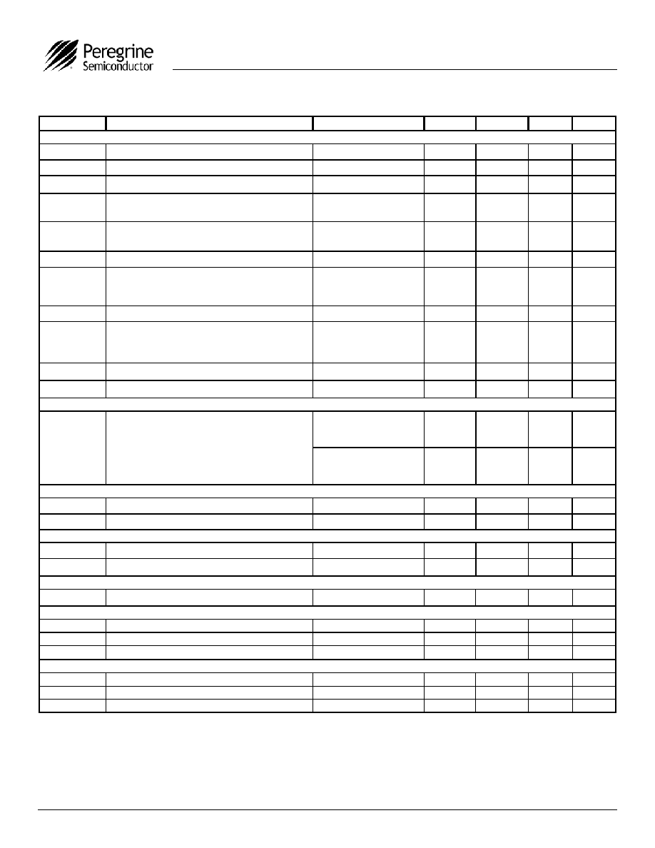
Table 6. AC Characteristics: VDD = 3.3 V, -40° C < TA < 85° C, unless otherwise specified
Note 1: Fclk is verified during the functional pattern test. Serial programming sections of the functional pattern are clocked at 10 MHz to verify Fclk
specification.
Note 2: CMOS logic levels can be used to drive reference input if DC coupled. Voltage input needs to be a minimum of 0.5Vp-p.
Note 3: Parameter is guaranteed through characterization only and is not tested.
Note 4: Parameters below are not tested for die sales. These parameters are verified during the element evaluation.
Symbol
Parameter
Conditions
Min
Typical
Max
Units
Control Interface and Latches (see Figures 4, 5, 6)
fClk
Serial data clock frequency
(Note 1)
10
MHz
tClkH
Serial clock HIGH time
30
ns
tClkL
Serial clock LOW time
30
ns
tDSU
Sdata set-up time after Sclk rising edge, D[7:0] set-up
time to M1_WR, M2_WR, A_WR, E_WR rising edge
10
ns
tDHLD
Sdata hold time after Sclk rising edge, D[7:0] hold
time to M1_WR, M2_WR, A_WR, E_WR rising edge
10
ns
tPW
S_WR, M1_WR, M2_WR, A_WR, E_WR pulse width
30
ns
tCWR
Sclk rising edge to S_WR rising edge. S_WR,
M1_WR, M2_WR, A_WR falling edge to Hop_WR
rising edge
30
ns
tCE
Sclk falling edge to E_WR transition
30
ns
tWRC
S_WR falling edge to Sclk rising edge. Hop_WR
falling edge to S_WR, M1_WR, M2_WR, A_WR rising
edge
30
ns
tEC
E_WR transition to Sclk rising edge
30
ns
tMDO
MSEL data out delay after Fin rising edge
CL = 12 pf
8
ns
Main Divider (Including Prescaler) (Note 4)
PFin
Input level range
External AC coupling
275 MHz
≤ Freq ≤ 3200MHz
-5
5
dBm
External AC coupling
3.2 GHz < Freq
≤ 3.5 GHz
3.15 V
≤ VDD ≤ 3.45 V
0
5
dBm
Main Divider (Prescaler Bypassed) (Note 4)
Fin
Operating frequency
50
300
MHz
PFin
Input level range
External AC coupling
-5
5
dBm
Reference Divider
fr
Operating frequency
(Note 3)
100
MHz
Pfr
Reference input power (Note 2)
Single-ended input
-2
10
dBm
Phase Detector
fc
Comparison frequency
(Note 3)
50
MHz
SSB Phase Noise (Fin = 1.9 GHz, fr = 20 MHz, fc = 20 MHz, LBW = 50 kHz, VDD = 3.3 V, Temp = 25
° C) (Note 4)
ΦN
Phase Noise
100 Hz Offset
-89
dBc/Hz
ΦN
Phase Noise
1 kHz Offset
-95
dBc/Hz
ΦN
Phase Noise
10 kHz Offset
-102
dBc/Hz
SSB Phase Noise (Fin = 1.9 GHz, fr = 20 MHz, fc = 20 MHz, LBW = 50 kHz, VDD = 3.0 V, Temp = 25
° C) (Note 4)
ΦN
Phase Noise
100 Hz Offset
-87
dBc/Hz
ΦN
Phase Noise
1 kHz Offset
-94
dBc/Hz
ΦN
Phase Noise
10 kHz Offset
-101
dBc/Hz
相关PDF资料 |
PDF描述 |
|---|---|
| PE33361MLIAA | PHASE LOCKED LOOP, QCC48 |
| PE3337-99 | PHASE LOCKED LOOP, UUC52 |
| PE33631MLIAA | PHASE DETECTOR, QCC64 |
| PE33631MLIAA-Z | PHASE DETECTOR, QCC64 |
| PG001M | STEPPER MOTOR CONTROLLER, 0.015 A, PDIP16 |
相关代理商/技术参数 |
参数描述 |
|---|---|
| PE33363LF | 制造商:PASTERNACK 制造商全称:Pasternack Enterprises, Inc. 功能描述:CABLE ASSEMBLY RG316/U SMC PLUG RIGHT ANGLE(LEAD FREE) |
| PE3336EK | 制造商:PEREGRINE 制造商全称:PEREGRINE 功能描述:3000 MHz UltraCMOS⑩ Integer-N PLL for Low Phase Noise Applications |
| PE33370LF | 制造商:PASTERNACK 制造商全称:Pasternack Enterprises, Inc. 功能描述:CABLE ASSEMBLY RG217/U HN MALE TO HN MALE(LEAD FREE) |
| PE33383 | 制造商:PASTERNACK 制造商全称:Pasternack Enterprises, Inc. 功能描述:CABLE ASSEMBLY RG316/U BNC MALE TO TNC MALE |
| PE3339 | 制造商:PEREGRINE 制造商全称:PEREGRINE 功能描述:3.0 GHz Integer-N PLL for Low Phase Noise Applications |
发布紧急采购,3分钟左右您将得到回复。