- 您现在的位置:买卖IC网 > PDF目录369994 > PF48F4400P0VBQ0 (INTEL CORP) Intel StrataFlash Embedded Memory PDF资料下载
参数资料
| 型号: | PF48F4400P0VBQ0 |
| 厂商: | INTEL CORP |
| 元件分类: | PROM |
| 英文描述: | Intel StrataFlash Embedded Memory |
| 中文描述: | 32M X 16 FLASH 1.8V PROM, 88 ns, PBGA88 |
| 封装: | 8 X 11 MM, 1.20 MM HEIGHT, LEAD FREE, SCSP-88 |
| 文件页数: | 21/102页 |
| 文件大小: | 1609K |
| 代理商: | PF48F4400P0VBQ0 |
第1页第2页第3页第4页第5页第6页第7页第8页第9页第10页第11页第12页第13页第14页第15页第16页第17页第18页第19页第20页当前第21页第22页第23页第24页第25页第26页第27页第28页第29页第30页第31页第32页第33页第34页第35页第36页第37页第38页第39页第40页第41页第42页第43页第44页第45页第46页第47页第48页第49页第50页第51页第52页第53页第54页第55页第56页第57页第58页第59页第60页第61页第62页第63页第64页第65页第66页第67页第68页第69页第70页第71页第72页第73页第74页第75页第76页第77页第78页第79页第80页第81页第82页第83页第84页第85页第86页第87页第88页第89页第90页第91页第92页第93页第94页第95页第96页第97页第98页第99页第100页第101页第102页
1-Gbit P30 Family
Datasheet
Intel StrataFlash
Embedded Memory (P30)
Order Number: 306666, Revision: 001
April 2005
21
VCCQ
Power
Output Power Supply:
Output-driver source voltage.
VSS
Power
Ground:
Connect to system ground. Do not float any VSS connection.
RFU
—
Reserved for Future Use:
Reserved by Intel for future device functionality and enhancement. These
should be treated in the same way as a Do Not Use (DU) signal.
DU
—
Do Not Use:
Do not connect to any other signal, or power supply; must be left floating.
NC
—
No Connect:
No internal connection; can be driven or floated.
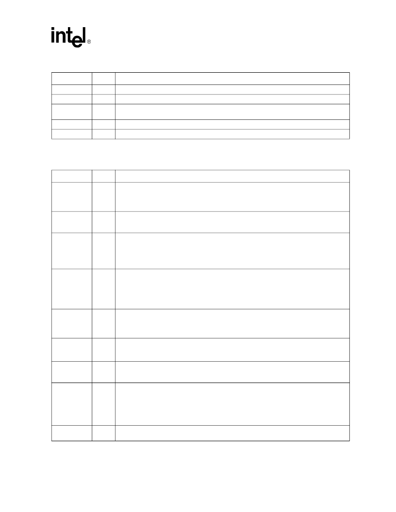
Table 3.
TSOP and Easy BGA Signal Descriptions (Sheet 2 of 2)
Symbol
Type
Name and Function
Table 4.
QUAD+ SCSP Signal Descriptions (Sheet 1 of 2)
Symbol
Type
Name and Function
A[MAX:0]
Input
ADDRESS INPUTS:
Device address inputs. 64-Mbit: A[21:0]; 128-Mbit: A[22:0]; 256-Mbit: A[23:0];
512-Mbit: A[24:0].
See
Table 6 on page 22
,
Figure 11 on page 23
, and
Figure 12 on page 23
for 512-Mbit and 1-Gbit
addressing.
DQ[15:0]
Input/
Output
DATA INPUT/OUTPUTS:
Inputs data and commands during write cycles; outputs data during
memory, Status Register, Protection Register, and Read Configuration Register reads. Data balls
float when the CE# or OE# are deasserted. Data is internally latched during writes.
ADV#
Input
ADDRESS VALID:
Active low input. During synchronous read operations, addresses are latched on
the rising edge of ADV#, or on the next valid CLK edge with ADV# low, whichever occurs first.
In asynchronous mode, the address is latched when ADV# going high or continuously flows through
if ADV# is held low.
WARNING: Designs not using ADV# must tie it to VSS to allow addresses to flow through.
F1-CE#
F2-CE#
Input
FLASH CHIP ENABLE:
Active low input. CE# low selects the associated flash memory die. When
asserted, flash internal control logic, input buffers, decoders, and sense amplifiers are active. When
deasserted, the associated flash die is deselected, power is reduced to standby levels, data and
WAIT outputs are placed in high-Z state.
See
Table 6 on page 22
for CE# assignment definitions.
WARNING: All chip enables must be high when device is not in use.
CLK
Input
CLOCK:
Synchronizes the device with the system’s bus frequency in synchronous-read mode.
During synchronous read operations, addresses are latched on the rising edge of ADV#, or on the
next valid CLK edge with ADV# low, whichever occurs first.
WARNING: Designs not using CLK for synchronous read mode must tie it to VCCQ or VSS.
F1-OE#
F2-OE#
Input
OUTPUT ENABLE:
Active low input. OE# low enables the device’s output data buffers during read
cycles. OE# high places the data outputs and WAIT in High-Z.
F1-OE# and F2-OE# should be tied together for all densities.
RST#
Input
RESET:
Active low input. RST# resets internal automation and inhibits write operations. This
provides data protection during power transitions. RST# high enables normal operation. Exit from
reset places the device in asynchronous read array mode.
WAIT
Output
WAIT:
Indicates data valid in synchronous array or non-array burst reads. Read Configuration
Register bit 10 (RCR[10], WT) determines its polarity when asserted. WAIT’s active output is V
OL
or
V
OH
when CE# and OE# are V
IL
. WAIT is high-Z if CE# or OE# is V
IH
.
In synchronous array or non-array read modes, WAIT indicates invalid data when asserted and
valid data when deasserted.
In asynchronous page mode, and all write modes, WAIT is deasserted.
WE#
Input
WRITE ENABLE:
Active low input. WE# controls writes to the device. Address and data are latched
on the rising edge of WE#.
相关PDF资料 |
PDF描述 |
|---|---|
| PF48F2000P0ZTQ0 | Intel StrataFlash Embedded Memory |
| PF48F3000P0ZTQ0 | Circular Connector; Body Material:Aluminum; Series:PT00; No. of Contacts:6; Connector Shell Size:10; Connecting Termination:Solder; Circular Shell Style:Wall Mount Receptacle; Circular Contact Gender:Pin; Insert Arrangement:10-6 |
| PF48F4000P0ZTQ0 | Circular Connector; MIL SPEC:MIL-C-26482, Series I, Solder; Body Material:Aluminum; Series:PT00; Number of Contacts:6; Connector Shell Size:10; Connecting Termination:Solder; Circular Shell Style:Wall Mount Receptacle |
| PF48F0P0ZTQ0 | Circular Connector; Body Material:Aluminum; Series:PT00; No. of Contacts:6; Connector Shell Size:10; Connecting Termination:Solder; Circular Shell Style:Wall Mount Receptacle; Circular Contact Gender:Socket; Insert Arrangement:10-98 |
| PF48F2P0ZTQ0 | Circular Connector; MIL SPEC:MIL-C-26482, Series I, Solder; Body Material:Aluminum; Series:PT00; No. of Contacts:10; Connector Shell Size:12; Connecting Termination:Solder; Circular Shell Style:Wall Mount Receptacle |
相关代理商/技术参数 |
参数描述 |
|---|---|
| PF48F4400P0VBQ0A | 功能描述:IC FLASH 512MBIT 85NS 88TPBGA RoHS:是 类别:集成电路 (IC) >> 存储器 系列:StrataFlash™ 产品变化通告:Product Discontinuation 26/Apr/2010 标准包装:136 系列:- 格式 - 存储器:RAM 存储器类型:SRAM - 同步,DDR II 存储容量:18M(1M x 18) 速度:200MHz 接口:并联 电源电压:1.7 V ~ 1.9 V 工作温度:0°C ~ 70°C 封装/外壳:165-TBGA 供应商设备封装:165-CABGA(13x15) 包装:托盘 其它名称:71P71804S200BQ |
| PF48F4400P0VBQ2E | 制造商:Micron Technology Inc 功能描述:32MX16 NOR FLASH PLASTIC PBF TFBGA 1.8V - Trays 制造商:Micron Technology Inc 功能描述:IC FLASH 512MBIT 85NS TFBGA |
| PF48F4400P0VBQ2F | 制造商:Micron Technology Inc 功能描述:32MX16 NOR FLASH PLASTIC PBF TFBGA 1.8V - Tape and Reel |
| PF48F4400P0VBQE0 | 功能描述:IC FLASH 512MBIT 100NS 88SCSP RoHS:是 类别:集成电路 (IC) >> 存储器 系列:Axcell™ 标准包装:576 系列:- 格式 - 存储器:闪存 存储器类型:闪存 - NAND 存储容量:512M(64M x 8) 速度:- 接口:并联 电源电压:2.7 V ~ 3.6 V 工作温度:-40°C ~ 85°C 封装/外壳:48-TFSOP(0.724",18.40mm 宽) 供应商设备封装:48-TSOP 包装:托盘 其它名称:497-5040 |
| PF48F4400P0VBQE3 | 功能描述:IC FLASH 512MBIT 100NS 88SCSP RoHS:是 类别:集成电路 (IC) >> 存储器 系列:Axcell™ 标准包装:576 系列:- 格式 - 存储器:闪存 存储器类型:闪存 - NAND 存储容量:512M(64M x 8) 速度:- 接口:并联 电源电压:2.7 V ~ 3.6 V 工作温度:-40°C ~ 85°C 封装/外壳:48-TFSOP(0.724",18.40mm 宽) 供应商设备封装:48-TSOP 包装:托盘 其它名称:497-5040 |
发布紧急采购,3分钟左右您将得到回复。