- 您现在的位置:买卖IC网 > PDF目录69043 > PGA117AIPW (TEXAS INSTRUMENTS INC) SPECIALTY ANALOG CIRCUIT, PDSO20 PDF资料下载
参数资料
| 型号: | PGA117AIPW |
| 厂商: | TEXAS INSTRUMENTS INC |
| 元件分类: | 模拟信号调理 |
| 英文描述: | SPECIALTY ANALOG CIRCUIT, PDSO20 |
| 封装: | GREEN, PLASTIC, TSSOP-20 |
| 文件页数: | 46/47页 |
| 文件大小: | 1545K |
| 代理商: | PGA117AIPW |
第1页第2页第3页第4页第5页第6页第7页第8页第9页第10页第11页第12页第13页第14页第15页第16页第17页第18页第19页第20页第21页第22页第23页第24页第25页第26页第27页第28页第29页第30页第31页第32页第33页第34页第35页第36页第37页第38页第39页第40页第41页第42页第43页第44页第45页当前第46页第47页
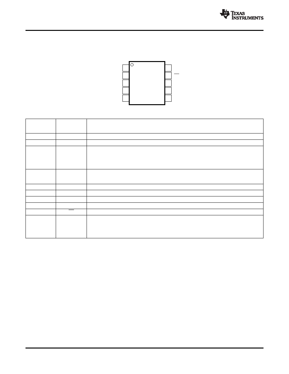
PIN CONFIGURATIONS
1
2
3
4
5
10
9
8
7
6
DV
DD
CS
DIO
SCLK
GND
AV
DD
CH1
V
/CH0
CAL
V
REF
V
OUT
PGA112
PGA113
SBOS424B – MARCH 2008 – REVISED SEPTEMBER 2008 ............................................................................................................................................ www.ti.com
MSOP-10
DGS PACKAGE
(TOP VIEW)
PGA112, PGA113 TERMINAL FUNCTIONS
MSOP
PACKAGE
PIN #
NAME
DESCRIPTION
1
AVDD
Analog supply voltage (+2.2V to +5.5V)
2
CH1
Input MUX channel 1
Input MUX channel 0 and VCAL input. For system calibration purposes, connect this pin to a
low-impedance external reference voltage to use internal calibration channels. The four internal
3
VCAL/CH0
calibration channels are connected to GND, 0.9VCAL, 0.1VCAL, and VREF, respectively. VCAL is loaded
with 100k
(typical) when internal calibration channels CAL2 or CAL3 are selected. Otherwise,
VCAL/CH0 appears as high impedance.
Reference input pin. Connect external reference for VOUT offset shift or to midsupply for midsupply
4
VREF
referenced systems. VREF must be connected to a low-impedance reference capable of sourcing and
sinking at least 2mA or VREF must be connected to GND.
5
VOUT
Analog voltage output. When AVDD < DVDD, VOUT is clamped to AVDD + 300mV.
6
GND
Ground pin
7
SCLK
Clock input for SPI serial interface
8
DIO
Data input/output for SPI serial interface. DIO contains a weak, 10
A internal pull-down current source.
9
CS
Chip select line for SPI serial interface
Digital and op amp output stage supply voltage (+2.2V to +5.5V). Useful in multi-supply systems to
prevent overvoltage/lockup condition on an analog-to-digital (ADC) input (for example, a microcontroller
10
DVDD
with an ADC running on +3V and the PGA powered from +5V). Digital I/O levels to be relative to DVDD.
DVDD should be bypassed with a 0.1F ceramic capacitor, and DVDD must supply the current for the
digital portion of the PGA as well as the load current for the op amp output stage.
8
Copyright 2008, Texas Instruments Incorporated
相关PDF资料 |
PDF描述 |
|---|---|
| PGA113AIDGSTG4 | SPECIALTY ANALOG CIRCUIT, PDSO10 |
| PGA113AIDGST | SPECIALTY ANALOG CIRCUIT, PDSO10 |
| PGA113AIDGSR | SPECIALTY ANALOG CIRCUIT, PDSO10 |
| PGA116AIPWG4 | SPECIALTY ANALOG CIRCUIT, PDSO20 |
| PGA117AIPWRG4 | SPECIALTY ANALOG CIRCUIT, PDSO20 |
相关代理商/技术参数 |
参数描述 |
|---|---|
| PGA117AIPWG4 | 功能描述:特殊用途放大器 Programmable Gain Amp w/Mux RoHS:否 制造商:Texas Instruments 通道数量:Single 共模抑制比(最小值): 输入补偿电压: 工作电源电压:3 V to 5.5 V 电源电流:5 mA 最大功率耗散: 最大工作温度:+ 70 C 最小工作温度:- 40 C 安装风格:SMD/SMT 封装 / 箱体:QFN-20 封装:Reel |
| PGA117AIPWR | 功能描述:特殊用途放大器 Zero-Drift Program Gain AMP/MUX RoHS:否 制造商:Texas Instruments 通道数量:Single 共模抑制比(最小值): 输入补偿电压: 工作电源电压:3 V to 5.5 V 电源电流:5 mA 最大功率耗散: 最大工作温度:+ 70 C 最小工作温度:- 40 C 安装风格:SMD/SMT 封装 / 箱体:QFN-20 封装:Reel |
| PGA117AIPWRG4 | 功能描述:特殊用途放大器 Programmable Gain Amp w/Mux RoHS:否 制造商:Texas Instruments 通道数量:Single 共模抑制比(最小值): 输入补偿电压: 工作电源电压:3 V to 5.5 V 电源电流:5 mA 最大功率耗散: 最大工作温度:+ 70 C 最小工作温度:- 40 C 安装风格:SMD/SMT 封装 / 箱体:QFN-20 封装:Reel |
| PGA-120-AH3-S-TG | 制造商:3M Electronic Products Division 功能描述: |
| PGA120M004B1-1315BLU | 制造商:FCI 功能描述: |
发布紧急采购,3分钟左右您将得到回复。