- 您现在的位置:买卖IC网 > PDF目录11610 > PIC12F1840T-I/MF (Microchip Technology)MCU 7KB FLASH 256B RAM XLP 8DFN PDF资料下载
参数资料
| 型号: | PIC12F1840T-I/MF |
| 厂商: | Microchip Technology |
| 文件页数: | 33/122页 |
| 文件大小: | 0K |
| 描述: | MCU 7KB FLASH 256B RAM XLP 8DFN |
| 标准包装: | 3,300 |
| 系列: | PIC® XLP™ 12F |
| 核心处理器: | PIC |
| 芯体尺寸: | 8-位 |
| 速度: | 32MHz |
| 连通性: | I²C,LIN,SPI,UART/USART |
| 外围设备: | 欠压检测/复位,POR,PWM,WDT |
| 输入/输出数: | 5 |
| 程序存储器容量: | 7KB(4K x 14) |
| 程序存储器类型: | 闪存 |
| EEPROM 大小: | 256 x 8 |
| RAM 容量: | 256 x 8 |
| 电压 - 电源 (Vcc/Vdd): | 2.3 V ~ 5.5 V |
| 数据转换器: | A/D 4x10b |
| 振荡器型: | 内部 |
| 工作温度: | -40°C ~ 85°C |
| 封装/外壳: | 8-VDFN 裸露焊盘 |
| 包装: | 带卷 (TR) |
第1页第2页第3页第4页第5页第6页第7页第8页第9页第10页第11页第12页第13页第14页第15页第16页第17页第18页第19页第20页第21页第22页第23页第24页第25页第26页第27页第28页第29页第30页第31页第32页当前第33页第34页第35页第36页第37页第38页第39页第40页第41页第42页第43页第44页第45页第46页第47页第48页第49页第50页第51页第52页第53页第54页第55页第56页第57页第58页第59页第60页第61页第62页第63页第64页第65页第66页第67页第68页第69页第70页第71页第72页第73页第74页第75页第76页第77页第78页第79页第80页第81页第82页第83页第84页第85页第86页第87页第88页第89页第90页第91页第92页第93页第94页第95页第96页第97页第98页第99页第100页第101页第102页第103页第104页第105页第106页第107页第108页第109页第110页第111页第112页第113页第114页第115页第116页第117页第118页第119页第120页第121页第122页
PIC12(L)F1840
DS41441B-page 18
Preliminary
2011 Microchip Technology Inc.
3.2.1.1
STATUS Register
The STATUS register, shown in Register 3-1, contains:
the arithmetic status of the ALU
the Reset status
The STATUS register can be the destination for any
instruction, like any other register. If the STATUS
register is the destination for an instruction that affects
the Z, DC or C bits, then the write to these three bits is
disabled. These bits are set or cleared according to the
device logic. Furthermore, the TO and PD bits are not
writable. Therefore, the result of an instruction with the
STATUS register as destination may be different than
intended.
For example, CLRF STATUS will clear the upper three
bits and set the Z bit. This leaves the STATUS register
as ‘000u u1uu’ (where u = unchanged).
It is recommended, therefore, that only BCF, BSF,
SWAPF
and MOVWF instructions are used to alter the
STATUS register, because these instructions do not
affect any Status bits. For other instructions not
affecting any Status bits (Refer to Section 29.0
).
Note 1:
The C and DC bits operate as Borrow
and Digit Borrow out bits, respectively, in
subtraction.
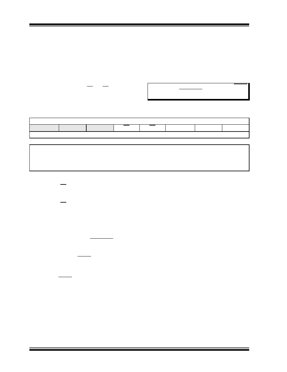
REGISTER 3-1:
STATUS: STATUS REGISTER
U-0
R-1/q
R/W-0/u
—
TO
PD
ZDC(1)
C(1)
bit 7
bit 0
Legend:
R = Readable bit
W = Writable bit
U = Unimplemented bit, read as ‘0’
u = Bit is unchanged
x = Bit is unknown
-n/n = Value at POR and BOR/Value at all other Resets
‘1’ = Bit is set
‘0’ = Bit is cleared
q = Value depends on condition
bit 7-5
Unimplemented:
Read as ‘0’
bit 4
TO:
Time-out bit
1
= After power-up, CLRWDT instruction or SLEEP instruction
0
= A WDT time-out occurred
bit 3
PD:
Power-down bit
1
= After power-up or by the CLRWDT instruction
0
= By execution of the SLEEP instruction
bit 2
Z:
Zero bit
1
= The result of an arithmetic or logic operation is zero
0
= The result of an arithmetic or logic operation is not zero
bit 1
DC:
Digit Carry/Digit Borrow bit(1)
1
= A carry-out from the 4th low-order bit of the result occurred
0
= No carry-out from the 4th low-order bit of the result
bit 0
C:
Carry/Borrow bit(1)
1
= A carry-out from the Most Significant bit of the result occurred
0
= No carry-out from the Most Significant bit of the result occurred
Note 1:
For Borrow, the polarity is reversed. A subtraction is executed by adding the two’s complement of the
second operand.
相关PDF资料 |
PDF描述 |
|---|---|
| VE-J3W-IW-F1 | CONVERTER MOD DC/DC 5.5V 100W |
| PIC16LF1903T-I/SS | MCU 7KB FLASH 256B RAM 28SSOP |
| VE-J3V-IW-F1 | CONVERTER MOD DC/DC 5.8V 100W |
| PIC16LF1902-E/SO | MCU 3.5KB FLASH 128B RAM 28SOIC |
| VE-J3P-IW-F3 | CONVERTER MOD DC/DC 13.8V 100W |
相关代理商/技术参数 |
参数描述 |
|---|---|
| PIC12F505 | 制造商:MICROCHIP 制造商全称:Microchip Technology 功能描述:8/14-Pin, 8-Bit Flash Microcontrollers |
| PIC12F505TE/MC | 制造商:MICROCHIP 制造商全称:Microchip Technology 功能描述:8/14-Pin, 8-Bit Flash Microcontrollers |
| PIC12F505TE/MG | 制造商:MICROCHIP 制造商全称:Microchip Technology 功能描述:8/14-Pin, 8-Bit Flash Microcontrollers |
| PIC12F505TE/MS | 制造商:MICROCHIP 制造商全称:Microchip Technology 功能描述:8/14-Pin, 8-Bit Flash Microcontrollers |
| PIC12F505TE/P | 制造商:MICROCHIP 制造商全称:Microchip Technology 功能描述:8/14-Pin, 8-Bit Flash Microcontrollers |
发布紧急采购,3分钟左右您将得到回复。