- 您现在的位置:买卖IC网 > PDF目录11610 > PIC12F1840T-I/MF (Microchip Technology)MCU 7KB FLASH 256B RAM XLP 8DFN PDF资料下载
参数资料
| 型号: | PIC12F1840T-I/MF |
| 厂商: | Microchip Technology |
| 文件页数: | 62/122页 |
| 文件大小: | 0K |
| 描述: | MCU 7KB FLASH 256B RAM XLP 8DFN |
| 标准包装: | 3,300 |
| 系列: | PIC® XLP™ 12F |
| 核心处理器: | PIC |
| 芯体尺寸: | 8-位 |
| 速度: | 32MHz |
| 连通性: | I²C,LIN,SPI,UART/USART |
| 外围设备: | 欠压检测/复位,POR,PWM,WDT |
| 输入/输出数: | 5 |
| 程序存储器容量: | 7KB(4K x 14) |
| 程序存储器类型: | 闪存 |
| EEPROM 大小: | 256 x 8 |
| RAM 容量: | 256 x 8 |
| 电压 - 电源 (Vcc/Vdd): | 2.3 V ~ 5.5 V |
| 数据转换器: | A/D 4x10b |
| 振荡器型: | 内部 |
| 工作温度: | -40°C ~ 85°C |
| 封装/外壳: | 8-VDFN 裸露焊盘 |
| 包装: | 带卷 (TR) |
第1页第2页第3页第4页第5页第6页第7页第8页第9页第10页第11页第12页第13页第14页第15页第16页第17页第18页第19页第20页第21页第22页第23页第24页第25页第26页第27页第28页第29页第30页第31页第32页第33页第34页第35页第36页第37页第38页第39页第40页第41页第42页第43页第44页第45页第46页第47页第48页第49页第50页第51页第52页第53页第54页第55页第56页第57页第58页第59页第60页第61页当前第62页第63页第64页第65页第66页第67页第68页第69页第70页第71页第72页第73页第74页第75页第76页第77页第78页第79页第80页第81页第82页第83页第84页第85页第86页第87页第88页第89页第90页第91页第92页第93页第94页第95页第96页第97页第98页第99页第100页第101页第102页第103页第104页第105页第106页第107页第108页第109页第110页第111页第112页第113页第114页第115页第116页第117页第118页第119页第120页第121页第122页
PIC12(L)F1840
DS41441B-page 44
Preliminary
2011 Microchip Technology Inc.
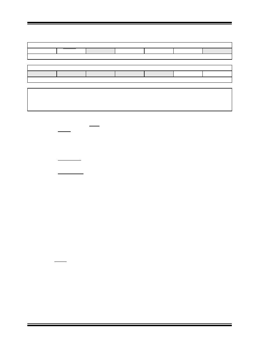
REGISTER 4-2:
CONFIGURATION WORD 2
R/P-1/1
U-1
R/P-1/1
U-1
LVP
DEBUG(2)
—
BORV
STVREN
PLLEN
—
bit 13
bit 7
U-1
R-1
U-1
R/P-1/1
—
Reserved
—
—WRT1
WRT0
bit 6
bit 0
Legend:
R = Readable bit
W = Writable bit
U = Unimplemented bit, read as ‘1’
u = Bit is unchanged
x = Bit is unknown
-n/n = Value at POR and BOR/Value at all other Resets
‘1’ = Bit is set
‘0’ = Bit is cleared
P = Programmable bit
bit 13
LVP:
Low-Voltage Programming Enable bit(1)
1
= Low-voltage programming enabled
0
= High-voltage on MCLR must be used for programming
bit 12
DEBUG:
In-Circuit Debugger Mode bit(2)
1
= In-Circuit Debugger disabled, ICSPCLK and ICSPDAT are general purpose I/O pins
0
= In-Circuit Debugger enabled, ICSPCLK and ICSPDAT are dedicated to the debugger
bit 11
Unimplemented:
Read as ‘1’
bit 10
BORV:
Brown-out Reset Voltage Selection bit
PIC12F1840:
1
= Brown-out Reset voltage set to 2.4V (typical)
0
= Brown-out Reset voltage set to 2.7V (typical)
PIC12LF1840:
1
= Brown-out Reset voltage set to 1.9V (typical)
0
= Brown-out Reset voltage set to 2.7V (typical)
bit 9
STVREN:
Stack Overflow/Underflow Reset Enable bit
1
= Stack Overflow or Underflow will cause a Reset
0
= Stack Overflow or Underflow will not cause a Reset
bit 8
PLLEN:
PLL Enable bit
1
= 4xPLL enabled
0
= 4xPLL disabled
bit 7-5
Unimplemented:
Read as ‘1’
bit 4
Reserved:
This location should be programmed to a ‘1’.
bit 3-2
Unimplemented:
Read as ‘1’
bit 1-0
WRT<1:0>:
Flash Memory Self-Write Protection bits
11
= Write protection off
10
= 000h to 1FFh write-protected, 200h to FFFh may be modified by EECON control
01
= 000h to 7FFh write-protected, 800h to FFFh may be modified by EECON control
00
= 000h to FFFh write-protected, no addresses may be modified by EECON control
Note
1:
The LVP bit cannot be programmed to ‘0’ when Programming mode is entered via LVP.
2:
The DEBUG bit in Configuration Word is managed automatically by device development tools including debuggers and
programmers. For normal device operation, this bit should be maintained as a '1'.
相关PDF资料 |
PDF描述 |
|---|---|
| VE-J3W-IW-F1 | CONVERTER MOD DC/DC 5.5V 100W |
| PIC16LF1903T-I/SS | MCU 7KB FLASH 256B RAM 28SSOP |
| VE-J3V-IW-F1 | CONVERTER MOD DC/DC 5.8V 100W |
| PIC16LF1902-E/SO | MCU 3.5KB FLASH 128B RAM 28SOIC |
| VE-J3P-IW-F3 | CONVERTER MOD DC/DC 13.8V 100W |
相关代理商/技术参数 |
参数描述 |
|---|---|
| PIC12F505 | 制造商:MICROCHIP 制造商全称:Microchip Technology 功能描述:8/14-Pin, 8-Bit Flash Microcontrollers |
| PIC12F505TE/MC | 制造商:MICROCHIP 制造商全称:Microchip Technology 功能描述:8/14-Pin, 8-Bit Flash Microcontrollers |
| PIC12F505TE/MG | 制造商:MICROCHIP 制造商全称:Microchip Technology 功能描述:8/14-Pin, 8-Bit Flash Microcontrollers |
| PIC12F505TE/MS | 制造商:MICROCHIP 制造商全称:Microchip Technology 功能描述:8/14-Pin, 8-Bit Flash Microcontrollers |
| PIC12F505TE/P | 制造商:MICROCHIP 制造商全称:Microchip Technology 功能描述:8/14-Pin, 8-Bit Flash Microcontrollers |
发布紧急采购,3分钟左右您将得到回复。