- 您现在的位置:买卖IC网 > PDF目录11401 > PIC16LC642-04/SP (Microchip Technology)IC MCU OTP 4KX14 COMP 28DIP PDF资料下载
参数资料
| 型号: | PIC16LC642-04/SP |
| 厂商: | Microchip Technology |
| 文件页数: | 56/125页 |
| 文件大小: | 0K |
| 描述: | IC MCU OTP 4KX14 COMP 28DIP |
| 产品培训模块: | Asynchronous Stimulus |
| 标准包装: | 15 |
| 系列: | PIC® 16C |
| 核心处理器: | PIC |
| 芯体尺寸: | 8-位 |
| 速度: | 4MHz |
| 外围设备: | 欠压检测/复位,LED,POR,WDT |
| 输入/输出数: | 22 |
| 程序存储器容量: | 7KB(4K x 14) |
| 程序存储器类型: | OTP |
| RAM 容量: | 176 x 8 |
| 电压 - 电源 (Vcc/Vdd): | 3 V ~ 6 V |
| 振荡器型: | 外部 |
| 工作温度: | 0°C ~ 70°C |
| 封装/外壳: | 28-DIP(0.300",7.62mm) |
| 包装: | 管件 |
第1页第2页第3页第4页第5页第6页第7页第8页第9页第10页第11页第12页第13页第14页第15页第16页第17页第18页第19页第20页第21页第22页第23页第24页第25页第26页第27页第28页第29页第30页第31页第32页第33页第34页第35页第36页第37页第38页第39页第40页第41页第42页第43页第44页第45页第46页第47页第48页第49页第50页第51页第52页第53页第54页第55页当前第56页第57页第58页第59页第60页第61页第62页第63页第64页第65页第66页第67页第68页第69页第70页第71页第72页第73页第74页第75页第76页第77页第78页第79页第80页第81页第82页第83页第84页第85页第86页第87页第88页第89页第90页第91页第92页第93页第94页第95页第96页第97页第98页第99页第100页第101页第102页第103页第104页第105页第106页第107页第108页第109页第110页第111页第112页第113页第114页第115页第116页第117页第118页第119页第120页第121页第122页第123页第124页第125页
Micrel, Inc.
KSZ8862-16/32MQL
April 2007
36
M9999-040407-3.0
Synchronous Interface
For synchronous transfers, the synchronous dedicated signals CYCLEN, SWR, and RDYRTNN will toggle but the
asynchronous dedicated signals RDN and WRN are de-asserted and stay at the same logic level throughout the entire
synchronous transfer.
The synchronous interface mainly supports two applications, one for VLBus-like and the other for EISA-like (DMA type C)
burst transfers. The VLBus-like interface supports only single-data transfer. The pin option VLBUSN determines if it is a
VLBus-like or EISA-like burst transfer – if VLBUSN = 0, the interface is for VLBus-like transfer; if VLBUSN = 1, the
interface is for EISA-like burst transfer.
For VLBus-like transfer interface (VLBUSN = 0):
This interface is used in an architecture in which the device’s local decoder is utilized; that is, the BIU decodes latched
A[15:4] and qualifies with AEN (Address Enable) to determine if the switch is the intended target. No burst is
supported in this application. The M/nIO signal connection in VLBus is routed to AEN. The CYCLEN in this application
is used to sample the SWR signal when it is asserted. Usually, CYCLEN is one clock delay of ADSN. There is a
handshaking process to end the cycle of VLBus-like transfers. When the KSZ8862M is ready to finish the cycle, it
asserts SRDYN
. The system/host acknowledges SRDYN by asserting RDYRTNN after the system/host has latched
the read data. The KSZ8862M holds the read data until RDYRTNN is asserted. The timing waveform is shown in
Figure 22 and Figure 23.
For EISA-like burst transfer interface (VLBUSN = 1):
The SWR is connected to IORC# in EISA to indicate the burst read and CYCLEN is connected to IOWC# in EISA to
indicate the burst write. Note that in this application, both the system/host/memory and KSZ8862M are capable of
inserting wait states. For system/host/memory to insert a wait state, assert the RDYRTNN signal; for the KSZ8862M
to insert the wait state, assert the SRDYN signal. The timing waveform is shown in Figure 20 and Figure 21.
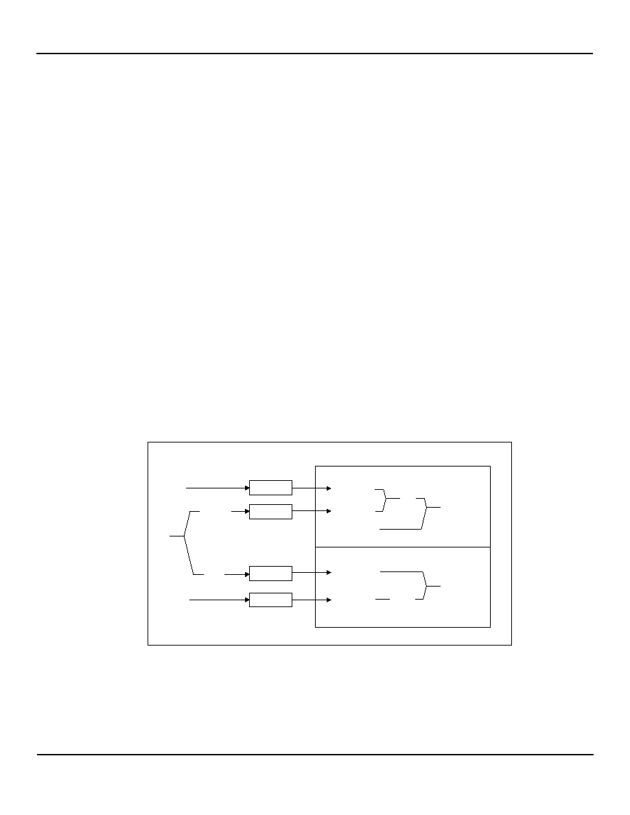
Summary
Figure 9 shows the mapping from ISA-like, EISA-like and VLBus-like transactions to the switch’s BIU.
Figure 10 shows the connection for different data bus sizes.
Note: For the 8-bit data bus mode, the internal inverter is enabled and connected between BE0N and BE1N, so even
address will enable the BE0N and odd address will enable the BE1N.
KSZ8862M BIU
Asynchronous
Interface
Synchronous
Interface
Address Latch
No Addr Latch
(ADSN = 0)
Central decode
Local
decode
Address Latch
Central decode
(VLBUSN = 1)
Local
decode
(VLBUSN = 0)
Host Logic
ISA
EISA
VLBus
Burst
Non-burst
Note: To use DATACSN & 32-bit only for Central decode
Figure 9. Mapping from ISA-like, EISA-like, and VLBus-like transactions to the KSZ8862M Bus
相关PDF资料 |
PDF描述 |
|---|---|
| VE-B4Y-IW | CONVERTER MOD DC/DC 3.3V 66W |
| PIC16LC642-04/SO | IC MCU OTP 4KX14 COMP 28SOIC |
| VE-B4X-IY | CONVERTER MOD DC/DC 5.2V 50W |
| PIC16C56-10/SS | IC MCU OTP 1KX12 20SSOP |
| VE-25B-CV-F2 | CONVERTER MOD DC/DC 95V 150W |
相关代理商/技术参数 |
参数描述 |
|---|---|
| PIC16LC642T-04/SO | 功能描述:8位微控制器 -MCU 7KB 176 RAM 22 I/O RoHS:否 制造商:Silicon Labs 核心:8051 处理器系列:C8051F39x 数据总线宽度:8 bit 最大时钟频率:50 MHz 程序存储器大小:16 KB 数据 RAM 大小:1 KB 片上 ADC:Yes 工作电源电压:1.8 V to 3.6 V 工作温度范围:- 40 C to + 105 C 封装 / 箱体:QFN-20 安装风格:SMD/SMT |
| PIC16LC642T-04I/SO | 功能描述:8位微控制器 -MCU 7KB 176 RAM 22 I/O RoHS:否 制造商:Silicon Labs 核心:8051 处理器系列:C8051F39x 数据总线宽度:8 bit 最大时钟频率:50 MHz 程序存储器大小:16 KB 数据 RAM 大小:1 KB 片上 ADC:Yes 工作电源电压:1.8 V to 3.6 V 工作温度范围:- 40 C to + 105 C 封装 / 箱体:QFN-20 安装风格:SMD/SMT |
| PIC16LC64A-04/L | 功能描述:8位微控制器 -MCU 3.5KB 128 RAM 33 I/O RoHS:否 制造商:Silicon Labs 核心:8051 处理器系列:C8051F39x 数据总线宽度:8 bit 最大时钟频率:50 MHz 程序存储器大小:16 KB 数据 RAM 大小:1 KB 片上 ADC:Yes 工作电源电压:1.8 V to 3.6 V 工作温度范围:- 40 C to + 105 C 封装 / 箱体:QFN-20 安装风格:SMD/SMT |
| PIC16LC64A-04/P | 功能描述:8位微控制器 -MCU 3.5KB 128 RAM 33 I/O RoHS:否 制造商:Silicon Labs 核心:8051 处理器系列:C8051F39x 数据总线宽度:8 bit 最大时钟频率:50 MHz 程序存储器大小:16 KB 数据 RAM 大小:1 KB 片上 ADC:Yes 工作电源电压:1.8 V to 3.6 V 工作温度范围:- 40 C to + 105 C 封装 / 箱体:QFN-20 安装风格:SMD/SMT |
| PIC16LC64A-04/PQ | 功能描述:8位微控制器 -MCU 3.5KB 128 RAM 33 I/O RoHS:否 制造商:Silicon Labs 核心:8051 处理器系列:C8051F39x 数据总线宽度:8 bit 最大时钟频率:50 MHz 程序存储器大小:16 KB 数据 RAM 大小:1 KB 片上 ADC:Yes 工作电源电压:1.8 V to 3.6 V 工作温度范围:- 40 C to + 105 C 封装 / 箱体:QFN-20 安装风格:SMD/SMT |
发布紧急采购,3分钟左右您将得到回复。