- 您现在的位置:买卖IC网 > PDF目录11401 > PIC16LC642-04/SP (Microchip Technology)IC MCU OTP 4KX14 COMP 28DIP PDF资料下载
参数资料
| 型号: | PIC16LC642-04/SP |
| 厂商: | Microchip Technology |
| 文件页数: | 57/125页 |
| 文件大小: | 0K |
| 描述: | IC MCU OTP 4KX14 COMP 28DIP |
| 产品培训模块: | Asynchronous Stimulus |
| 标准包装: | 15 |
| 系列: | PIC® 16C |
| 核心处理器: | PIC |
| 芯体尺寸: | 8-位 |
| 速度: | 4MHz |
| 外围设备: | 欠压检测/复位,LED,POR,WDT |
| 输入/输出数: | 22 |
| 程序存储器容量: | 7KB(4K x 14) |
| 程序存储器类型: | OTP |
| RAM 容量: | 176 x 8 |
| 电压 - 电源 (Vcc/Vdd): | 3 V ~ 6 V |
| 振荡器型: | 外部 |
| 工作温度: | 0°C ~ 70°C |
| 封装/外壳: | 28-DIP(0.300",7.62mm) |
| 包装: | 管件 |
第1页第2页第3页第4页第5页第6页第7页第8页第9页第10页第11页第12页第13页第14页第15页第16页第17页第18页第19页第20页第21页第22页第23页第24页第25页第26页第27页第28页第29页第30页第31页第32页第33页第34页第35页第36页第37页第38页第39页第40页第41页第42页第43页第44页第45页第46页第47页第48页第49页第50页第51页第52页第53页第54页第55页第56页当前第57页第58页第59页第60页第61页第62页第63页第64页第65页第66页第67页第68页第69页第70页第71页第72页第73页第74页第75页第76页第77页第78页第79页第80页第81页第82页第83页第84页第85页第86页第87页第88页第89页第90页第91页第92页第93页第94页第95页第96页第97页第98页第99页第100页第101页第102页第103页第104页第105页第106页第107页第108页第109页第110页第111页第112页第113页第114页第115页第116页第117页第118页第119页第120页第121页第122页第123页第124页第125页
Micrel, Inc.
KSZ8862-16/32MQL
April 2007
37
M9999-040407-3.0
D[7:0]
D[15:8]
D[23:16]
D[31:24]
GND
HD[7:0]
nHBE[0]
nHBE[2]
nHBE[3]
HD[15:8]
nHBE[1]
HD[23:16]
HD[31:24]
A[15:2]
A[1]
D[7:0]
D[15:8]
BE0N
BE1N
8-bit Data Bus
HA[1]
HA[15:2]
HD[7:0]
HA[0]
VDD
A[15:2]
A[1]
D[7:0]
D[15:8]
BE0N
BE1N
16-bit Data Bus
(for example: ISA-like)
HA[1]
HA[15:2]
HD[7:0]
HA[0]
nSBHE
A[15:2]
A[1]
BE0N
BE1N
BE2N
BE3N
32-bit Data Bus
(for example: EISA-like)
HA[15:2]
HD[15:8]
KSZ8862-16
KSZ8862-32
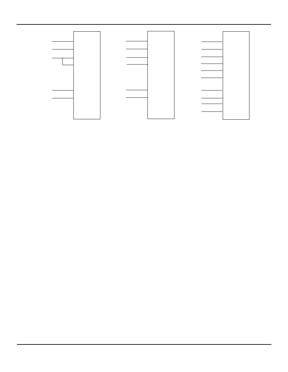
Figure 10. KSZ8862M 8-Bit, 16-Bit, and 32-Bit Data Bus Connections
BIU Implementation Principles
Since the KSZ8862M is an I/O device with 16 addressable locations, address decoding is based on the values of A15-A4
and AEN. Whenever DATACSN is asserted, the address decoder is disabled and a 32-bit transfer to Data Register is
assumed (BE3N – BE0N are ignored).
If address latching is required, the address is latched on the rising edge of ADSN and is transparent when ADSN=0.
1.
Byte, word, and double-word data buses and accesses (transfers) are supported.
2.
Internal byte swapping is not implemented and word swapping is supported internally. Refer to Figure 12 for the
appropriate 8-bit, 16-bit, and 32-bit data bus connection.
3.
Since independent sets of synchronous and asynchronous signals are provided, synchronous and asynchronous
cycles can be mixed or interleaved as long as they are not active simultaneously.
4.
The asynchronous interface uses RDN and WRN signal strobes for data latching. If necessary, ARDY is de-
asserted on the leading edge of the strobe.
5.
The VLBUS-like synchronous interface uses BCLK, ADSN, and SWR and CYCLEN to control read and write
operations and generate SRDYN to insert the wait state, if necessary, when VLBUSN = 0. For read, the data must
be held until RDYRTNN is asserted.
6.
The EISA-like burst transfer is supported using synchronous interface signals and DATACSN when I/O signal
VLBUSN = 1. Both the system/host/memory and KSZ8862M are capable of inserting wait states. To set the
system/host/memory to insert a wait state, assert RDYRTNN signal. To set the KSZ8862M to insert a wait state,
assert SRDYN signal.
相关PDF资料 |
PDF描述 |
|---|---|
| VE-B4Y-IW | CONVERTER MOD DC/DC 3.3V 66W |
| PIC16LC642-04/SO | IC MCU OTP 4KX14 COMP 28SOIC |
| VE-B4X-IY | CONVERTER MOD DC/DC 5.2V 50W |
| PIC16C56-10/SS | IC MCU OTP 1KX12 20SSOP |
| VE-25B-CV-F2 | CONVERTER MOD DC/DC 95V 150W |
相关代理商/技术参数 |
参数描述 |
|---|---|
| PIC16LC642T-04/SO | 功能描述:8位微控制器 -MCU 7KB 176 RAM 22 I/O RoHS:否 制造商:Silicon Labs 核心:8051 处理器系列:C8051F39x 数据总线宽度:8 bit 最大时钟频率:50 MHz 程序存储器大小:16 KB 数据 RAM 大小:1 KB 片上 ADC:Yes 工作电源电压:1.8 V to 3.6 V 工作温度范围:- 40 C to + 105 C 封装 / 箱体:QFN-20 安装风格:SMD/SMT |
| PIC16LC642T-04I/SO | 功能描述:8位微控制器 -MCU 7KB 176 RAM 22 I/O RoHS:否 制造商:Silicon Labs 核心:8051 处理器系列:C8051F39x 数据总线宽度:8 bit 最大时钟频率:50 MHz 程序存储器大小:16 KB 数据 RAM 大小:1 KB 片上 ADC:Yes 工作电源电压:1.8 V to 3.6 V 工作温度范围:- 40 C to + 105 C 封装 / 箱体:QFN-20 安装风格:SMD/SMT |
| PIC16LC64A-04/L | 功能描述:8位微控制器 -MCU 3.5KB 128 RAM 33 I/O RoHS:否 制造商:Silicon Labs 核心:8051 处理器系列:C8051F39x 数据总线宽度:8 bit 最大时钟频率:50 MHz 程序存储器大小:16 KB 数据 RAM 大小:1 KB 片上 ADC:Yes 工作电源电压:1.8 V to 3.6 V 工作温度范围:- 40 C to + 105 C 封装 / 箱体:QFN-20 安装风格:SMD/SMT |
| PIC16LC64A-04/P | 功能描述:8位微控制器 -MCU 3.5KB 128 RAM 33 I/O RoHS:否 制造商:Silicon Labs 核心:8051 处理器系列:C8051F39x 数据总线宽度:8 bit 最大时钟频率:50 MHz 程序存储器大小:16 KB 数据 RAM 大小:1 KB 片上 ADC:Yes 工作电源电压:1.8 V to 3.6 V 工作温度范围:- 40 C to + 105 C 封装 / 箱体:QFN-20 安装风格:SMD/SMT |
| PIC16LC64A-04/PQ | 功能描述:8位微控制器 -MCU 3.5KB 128 RAM 33 I/O RoHS:否 制造商:Silicon Labs 核心:8051 处理器系列:C8051F39x 数据总线宽度:8 bit 最大时钟频率:50 MHz 程序存储器大小:16 KB 数据 RAM 大小:1 KB 片上 ADC:Yes 工作电源电压:1.8 V to 3.6 V 工作温度范围:- 40 C to + 105 C 封装 / 箱体:QFN-20 安装风格:SMD/SMT |
发布紧急采购,3分钟左右您将得到回复。