- 您现在的位置:买卖IC网 > PDF目录11515 > PIC16LF72T-I/ML (Microchip Technology)IC MCU FLASH 2KX14 LV AD 28-QFN PDF资料下载
参数资料
| 型号: | PIC16LF72T-I/ML |
| 厂商: | Microchip Technology |
| 文件页数: | 128/136页 |
| 文件大小: | 0K |
| 描述: | IC MCU FLASH 2KX14 LV AD 28-QFN |
| 产品培训模块: | Asynchronous Stimulus |
| 标准包装: | 1,600 |
| 系列: | PIC® 16F |
| 核心处理器: | PIC |
| 芯体尺寸: | 8-位 |
| 速度: | 20MHz |
| 连通性: | I²C,SPI |
| 外围设备: | 欠压检测/复位,POR,PWM,WDT |
| 输入/输出数: | 22 |
| 程序存储器容量: | 3.5KB(2K x 14) |
| 程序存储器类型: | 闪存 |
| RAM 容量: | 128 x 8 |
| 电压 - 电源 (Vcc/Vdd): | 2 V ~ 5.5 V |
| 数据转换器: | A/D 5x8b |
| 振荡器型: | 外部 |
| 工作温度: | -40°C ~ 85°C |
| 封装/外壳: | 28-VQFN 裸露焊盘 |
| 包装: | 带卷 (TR) |
第1页第2页第3页第4页第5页第6页第7页第8页第9页第10页第11页第12页第13页第14页第15页第16页第17页第18页第19页第20页第21页第22页第23页第24页第25页第26页第27页第28页第29页第30页第31页第32页第33页第34页第35页第36页第37页第38页第39页第40页第41页第42页第43页第44页第45页第46页第47页第48页第49页第50页第51页第52页第53页第54页第55页第56页第57页第58页第59页第60页第61页第62页第63页第64页第65页第66页第67页第68页第69页第70页第71页第72页第73页第74页第75页第76页第77页第78页第79页第80页第81页第82页第83页第84页第85页第86页第87页第88页第89页第90页第91页第92页第93页第94页第95页第96页第97页第98页第99页第100页第101页第102页第103页第104页第105页第106页第107页第108页第109页第110页第111页第112页第113页第114页第115页第116页第117页第118页第119页第120页第121页第122页第123页第124页第125页第126页第127页当前第128页第129页第130页第131页第132页第133页第134页第135页第136页
91
2535J–AVR–08/10
ATtiny13
Quantization Error: Due to the quantization of the input voltage into a finite number of codes,
a range of input voltages (1 LSB wide) will code to the same value. Always ± 0.5 LSB.
Absolute Accuracy: The maximum deviation of an actual (unadjusted) transition compared to
an ideal transition for any code. This is the compound effect of offset, gain error, differential
error, non-linearity, and quantization error. Ideal value: ± 0.5 LSB.
14.11 ADC Conversion Result
After the conversion is complete (ADIF is high), the conversion result can be found in the ADC
Result Registers (ADCL, ADCH).
For single ended conversion, the result is
where VIN is the voltage on the selected input pin and VREF the selected voltage reference (see
Table 14-2 on page 91 and Table 14-3 on page 92). 0x000 represents analog ground, and
0x3FF represents the selected reference voltage minus one LSB.
14.12 Register Description
14.12.1
ADMUX – ADC Multiplexer Selection Register
Bit 7 – Res: Reserved Bit
This bit is reserved bit in the ATtiny13 and will always read as zero.
Bit 6 – REFS0: Reference Selection Bit
This bit selects the voltage reference for the ADC, as shown in Table 14-2. If this bit is changed
during a conversion, the change will not go in effect until this conversion is complete (ADIF in
ADCSRA is set).
Bit 5 – ADLAR: ADC Left Adjust Result
The ADLAR bit affects the presentation of the ADC conversion result in the ADC Data Register.
Write one to ADLAR to left adjust the result. Otherwise, the result is right adjusted. Changing the
ADLAR bit will affect the ADC Data Register immediately, regardless of any ongoing conver-
sions. For a complete description of this bit, see “ADCL and ADCH – The ADC Data Register” on
ADC
VIN 1024
VREF
--------------------------
=
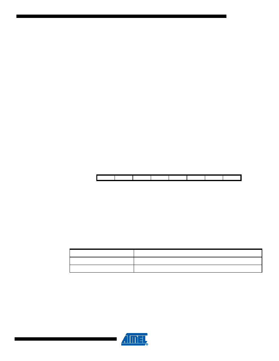
Bit
7
65432
10
–
REFS0
ADLAR
–
MUX1
MUX0
ADMUX
Read/Write
R
R/W
R
R/W
Initial Value
0
00000
00
Table 14-2.
Voltage Reference Selections for ADC
REFS0
Voltage Reference Selection
0VCC used as analog reference.
1
Internal Voltage Reference.
相关PDF资料 |
PDF描述 |
|---|---|
| VI-JTH-IX-S | CONVERTER MOD DC/DC 52V 75W |
| VE-203-IY-B1 | CONVERTER MOD DC/DC 24V 50W |
| VI-JT3-IX-S | CONVERTER MOD DC/DC 24V 75W |
| PIC16LF72-I/SS | IC PIC MCU FLASH 2KX14 28SSOP |
| VI-J74-IX-S | CONVERTER MOD DC/DC 48V 75W |
相关代理商/技术参数 |
参数描述 |
|---|---|
| PIC16LF737-I/ML | 功能描述:8位微控制器 -MCU 7KB 368 RAM 25 I/O RoHS:否 制造商:Silicon Labs 核心:8051 处理器系列:C8051F39x 数据总线宽度:8 bit 最大时钟频率:50 MHz 程序存储器大小:16 KB 数据 RAM 大小:1 KB 片上 ADC:Yes 工作电源电压:1.8 V to 3.6 V 工作温度范围:- 40 C to + 105 C 封装 / 箱体:QFN-20 安装风格:SMD/SMT |
| PIC16LF737-I/SO | 功能描述:8位微控制器 -MCU 7KB 368 RAM 25 I/O RoHS:否 制造商:Silicon Labs 核心:8051 处理器系列:C8051F39x 数据总线宽度:8 bit 最大时钟频率:50 MHz 程序存储器大小:16 KB 数据 RAM 大小:1 KB 片上 ADC:Yes 工作电源电压:1.8 V to 3.6 V 工作温度范围:- 40 C to + 105 C 封装 / 箱体:QFN-20 安装风格:SMD/SMT |
| PIC16LF737-I/SP | 功能描述:8位微控制器 -MCU 7KB 368 RAM 25 I/O RoHS:否 制造商:Silicon Labs 核心:8051 处理器系列:C8051F39x 数据总线宽度:8 bit 最大时钟频率:50 MHz 程序存储器大小:16 KB 数据 RAM 大小:1 KB 片上 ADC:Yes 工作电源电压:1.8 V to 3.6 V 工作温度范围:- 40 C to + 105 C 封装 / 箱体:QFN-20 安装风格:SMD/SMT |
| PIC16LF737-I/SS | 功能描述:8位微控制器 -MCU 7KB 368 RAM 25 I/O RoHS:否 制造商:Silicon Labs 核心:8051 处理器系列:C8051F39x 数据总线宽度:8 bit 最大时钟频率:50 MHz 程序存储器大小:16 KB 数据 RAM 大小:1 KB 片上 ADC:Yes 工作电源电压:1.8 V to 3.6 V 工作温度范围:- 40 C to + 105 C 封装 / 箱体:QFN-20 安装风格:SMD/SMT |
| PIC16LF737T-I/ML | 功能描述:8位微控制器 -MCU 7KB 368 RAM 25 I/O RoHS:否 制造商:Silicon Labs 核心:8051 处理器系列:C8051F39x 数据总线宽度:8 bit 最大时钟频率:50 MHz 程序存储器大小:16 KB 数据 RAM 大小:1 KB 片上 ADC:Yes 工作电源电压:1.8 V to 3.6 V 工作温度范围:- 40 C to + 105 C 封装 / 箱体:QFN-20 安装风格:SMD/SMT |
发布紧急采购,3分钟左右您将得到回复。