- 您现在的位置:买卖IC网 > PDF目录11515 > PIC16LF72T-I/ML (Microchip Technology)IC MCU FLASH 2KX14 LV AD 28-QFN PDF资料下载
参数资料
| 型号: | PIC16LF72T-I/ML |
| 厂商: | Microchip Technology |
| 文件页数: | 63/136页 |
| 文件大小: | 0K |
| 描述: | IC MCU FLASH 2KX14 LV AD 28-QFN |
| 产品培训模块: | Asynchronous Stimulus |
| 标准包装: | 1,600 |
| 系列: | PIC® 16F |
| 核心处理器: | PIC |
| 芯体尺寸: | 8-位 |
| 速度: | 20MHz |
| 连通性: | I²C,SPI |
| 外围设备: | 欠压检测/复位,POR,PWM,WDT |
| 输入/输出数: | 22 |
| 程序存储器容量: | 3.5KB(2K x 14) |
| 程序存储器类型: | 闪存 |
| RAM 容量: | 128 x 8 |
| 电压 - 电源 (Vcc/Vdd): | 2 V ~ 5.5 V |
| 数据转换器: | A/D 5x8b |
| 振荡器型: | 外部 |
| 工作温度: | -40°C ~ 85°C |
| 封装/外壳: | 28-VQFN 裸露焊盘 |
| 包装: | 带卷 (TR) |
第1页第2页第3页第4页第5页第6页第7页第8页第9页第10页第11页第12页第13页第14页第15页第16页第17页第18页第19页第20页第21页第22页第23页第24页第25页第26页第27页第28页第29页第30页第31页第32页第33页第34页第35页第36页第37页第38页第39页第40页第41页第42页第43页第44页第45页第46页第47页第48页第49页第50页第51页第52页第53页第54页第55页第56页第57页第58页第59页第60页第61页第62页当前第63页第64页第65页第66页第67页第68页第69页第70页第71页第72页第73页第74页第75页第76页第77页第78页第79页第80页第81页第82页第83页第84页第85页第86页第87页第88页第89页第90页第91页第92页第93页第94页第95页第96页第97页第98页第99页第100页第101页第102页第103页第104页第105页第106页第107页第108页第109页第110页第111页第112页第113页第114页第115页第116页第117页第118页第119页第120页第121页第122页第123页第124页第125页第126页第127页第128页第129页第130页第131页第132页第133页第134页第135页第136页
PIC16F72
DS39597C-page 30
2007 Microchip Technology Inc.
5.2
Timer1 Operation in Timer Mode
Timer mode is selected by clearing the TMR1CS
(T1CON<1>) bit. In this mode, the input clock to the
timer is FOSC/4. The synchronize control bit T1SYNC
(T1CON<2>) has no effect, since the internal clock is
always in sync.
5.3
Timer1 Counter Operation
Timer1 may operate in Asynchronous or Synchronous
mode, depending on the setting of the TMR1CS bit.
When Timer1 is being incremented via an external
source, increments occur on a rising edge. After Timer1
is enabled in Counter mode, the module must first have
a falling edge before the counter begins to increment.
5.4
Timer1 Operation in Synchronized
Counter Mode
Counter mode is selected by setting bit TMR1CS. In
this mode, the timer increments on every rising edge of
clock input on pin RC1/T1OSI when bit T1OSCEN is
set, or on pin RC0/T1OSO/T1CKI when bit T1OSCEN
is cleared.
If T1SYNC is cleared, then the external clock input is
synchronized with internal phase clocks. The synchro-
nization is done after the prescaler stage. The
prescaler stage is an asynchronous ripple counter.
In this configuration, during SLEEP mode, Timer1 will
not increment even if the external clock is present,
since the synchronization circuit is shut-off. The
prescaler, however, will continue to increment.
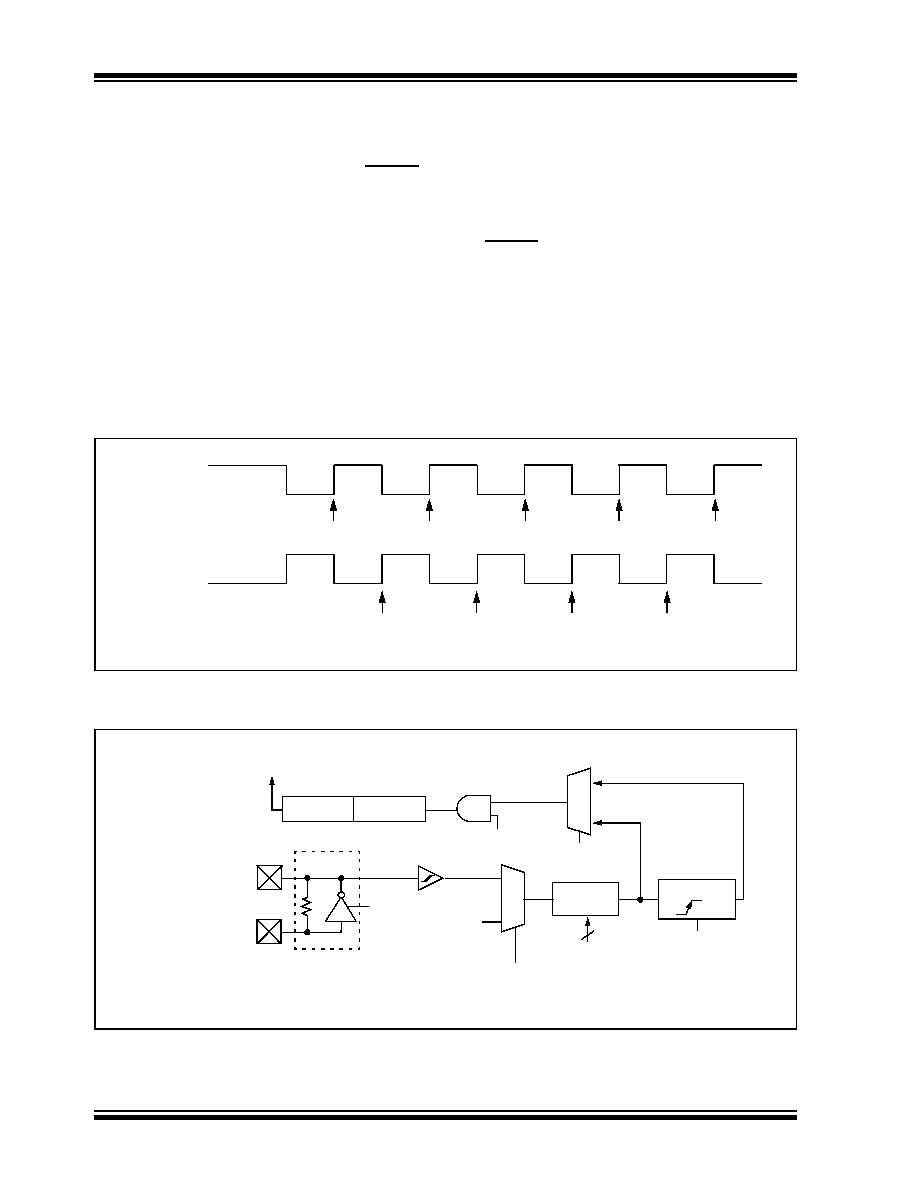
FIGURE 5-1:
TIMER1 INCREMENTING EDGE
FIGURE 5-2:
TIMER1 BLOCK DIAGRAM
T1CKI
(Default High)
T1CKI
(Default Low)
Note: Arrows indicate counter increments.
TMR1H
TMR1L
T1OSC
T1SYNC
TMR1CS
T1CKPS1:T1CKPS0
Q Clock
T1OSCEN
Enable
Oscillator(1)
FOSC/4
Internal
Clock
TMR1ON
On/Off
Prescaler
1, 2, 4, 8
Synchronize
det
1
0
1
Synchronized
Clock Input
2
RC0/T1OSO/T1CKI
RC1/T1OSI
Note
1: When the T1OSCEN bit is cleared, the inverter is turned off. This eliminates power drain.
Set Flag bit
TMR1IF on
Overflow
TMR1
(2)
相关PDF资料 |
PDF描述 |
|---|---|
| VI-JTH-IX-S | CONVERTER MOD DC/DC 52V 75W |
| VE-203-IY-B1 | CONVERTER MOD DC/DC 24V 50W |
| VI-JT3-IX-S | CONVERTER MOD DC/DC 24V 75W |
| PIC16LF72-I/SS | IC PIC MCU FLASH 2KX14 28SSOP |
| VI-J74-IX-S | CONVERTER MOD DC/DC 48V 75W |
相关代理商/技术参数 |
参数描述 |
|---|---|
| PIC16LF737-I/ML | 功能描述:8位微控制器 -MCU 7KB 368 RAM 25 I/O RoHS:否 制造商:Silicon Labs 核心:8051 处理器系列:C8051F39x 数据总线宽度:8 bit 最大时钟频率:50 MHz 程序存储器大小:16 KB 数据 RAM 大小:1 KB 片上 ADC:Yes 工作电源电压:1.8 V to 3.6 V 工作温度范围:- 40 C to + 105 C 封装 / 箱体:QFN-20 安装风格:SMD/SMT |
| PIC16LF737-I/SO | 功能描述:8位微控制器 -MCU 7KB 368 RAM 25 I/O RoHS:否 制造商:Silicon Labs 核心:8051 处理器系列:C8051F39x 数据总线宽度:8 bit 最大时钟频率:50 MHz 程序存储器大小:16 KB 数据 RAM 大小:1 KB 片上 ADC:Yes 工作电源电压:1.8 V to 3.6 V 工作温度范围:- 40 C to + 105 C 封装 / 箱体:QFN-20 安装风格:SMD/SMT |
| PIC16LF737-I/SP | 功能描述:8位微控制器 -MCU 7KB 368 RAM 25 I/O RoHS:否 制造商:Silicon Labs 核心:8051 处理器系列:C8051F39x 数据总线宽度:8 bit 最大时钟频率:50 MHz 程序存储器大小:16 KB 数据 RAM 大小:1 KB 片上 ADC:Yes 工作电源电压:1.8 V to 3.6 V 工作温度范围:- 40 C to + 105 C 封装 / 箱体:QFN-20 安装风格:SMD/SMT |
| PIC16LF737-I/SS | 功能描述:8位微控制器 -MCU 7KB 368 RAM 25 I/O RoHS:否 制造商:Silicon Labs 核心:8051 处理器系列:C8051F39x 数据总线宽度:8 bit 最大时钟频率:50 MHz 程序存储器大小:16 KB 数据 RAM 大小:1 KB 片上 ADC:Yes 工作电源电压:1.8 V to 3.6 V 工作温度范围:- 40 C to + 105 C 封装 / 箱体:QFN-20 安装风格:SMD/SMT |
| PIC16LF737T-I/ML | 功能描述:8位微控制器 -MCU 7KB 368 RAM 25 I/O RoHS:否 制造商:Silicon Labs 核心:8051 处理器系列:C8051F39x 数据总线宽度:8 bit 最大时钟频率:50 MHz 程序存储器大小:16 KB 数据 RAM 大小:1 KB 片上 ADC:Yes 工作电源电压:1.8 V to 3.6 V 工作温度范围:- 40 C to + 105 C 封装 / 箱体:QFN-20 安装风格:SMD/SMT |
发布紧急采购,3分钟左右您将得到回复。