- 您现在的位置:买卖IC网 > PDF目录11515 > PIC16LF72T-I/ML (Microchip Technology)IC MCU FLASH 2KX14 LV AD 28-QFN PDF资料下载
参数资料
| 型号: | PIC16LF72T-I/ML |
| 厂商: | Microchip Technology |
| 文件页数: | 92/136页 |
| 文件大小: | 0K |
| 描述: | IC MCU FLASH 2KX14 LV AD 28-QFN |
| 产品培训模块: | Asynchronous Stimulus |
| 标准包装: | 1,600 |
| 系列: | PIC® 16F |
| 核心处理器: | PIC |
| 芯体尺寸: | 8-位 |
| 速度: | 20MHz |
| 连通性: | I²C,SPI |
| 外围设备: | 欠压检测/复位,POR,PWM,WDT |
| 输入/输出数: | 22 |
| 程序存储器容量: | 3.5KB(2K x 14) |
| 程序存储器类型: | 闪存 |
| RAM 容量: | 128 x 8 |
| 电压 - 电源 (Vcc/Vdd): | 2 V ~ 5.5 V |
| 数据转换器: | A/D 5x8b |
| 振荡器型: | 外部 |
| 工作温度: | -40°C ~ 85°C |
| 封装/外壳: | 28-VQFN 裸露焊盘 |
| 包装: | 带卷 (TR) |
第1页第2页第3页第4页第5页第6页第7页第8页第9页第10页第11页第12页第13页第14页第15页第16页第17页第18页第19页第20页第21页第22页第23页第24页第25页第26页第27页第28页第29页第30页第31页第32页第33页第34页第35页第36页第37页第38页第39页第40页第41页第42页第43页第44页第45页第46页第47页第48页第49页第50页第51页第52页第53页第54页第55页第56页第57页第58页第59页第60页第61页第62页第63页第64页第65页第66页第67页第68页第69页第70页第71页第72页第73页第74页第75页第76页第77页第78页第79页第80页第81页第82页第83页第84页第85页第86页第87页第88页第89页第90页第91页当前第92页第93页第94页第95页第96页第97页第98页第99页第100页第101页第102页第103页第104页第105页第106页第107页第108页第109页第110页第111页第112页第113页第114页第115页第116页第117页第118页第119页第120页第121页第122页第123页第124页第125页第126页第127页第128页第129页第130页第131页第132页第133页第134页第135页第136页
2007 Microchip Technology Inc.
DS39597C-page 57
PIC16F72
10.5
A/D Operation During SLEEP
The A/D module can operate during SLEEP mode. This
requires that the A/D clock source be set to RC
(ADCS1:ADCS0 = 11). When the RC clock source is
selected, the A/D module waits one instruction cycle
before starting the conversion. This allows the SLEEP
instruction to be executed, which eliminates all digital
switching noise from the conversion. When the conver-
sion is completed, the GO/DONE bit will be cleared,
and the result loaded into the ADRES register. If the
A/D interrupt is enabled, the device will wake-up from
SLEEP. If the A/D interrupt is not enabled, the A/D mod-
ule will then be turned off, although the ADON bit will
remain set.
When the A/D clock source is another clock option (not
RC), a SLEEP instruction will cause the present conver-
sion to be aborted and the A/D module to be turned off,
though the ADON bit will remain set.
Turning off the A/D places the A/D module in its lowest
current consumption state.
10.6
Effects of a RESET
A device RESET forces all registers to their RESET
state. The A/D module is disabled and any conversion
in progress is aborted. All A/D input pins are configured
as analog inputs.
The ADRES register will contain unknown data after a
Power-on Reset.
10.7
Use of the CCP Trigger
An A/D conversion can be started by the “special event
trigger” of the CCP1 module. This requires that the
CCP1M3:CCP1M0 bits (CCP1CON<3:0>) be pro-
grammed as 1011 and that the A/D module is enabled
(ADON bit is set). When the trigger occurs, the
GO/DONE bit will be set, starting the A/D conversion,
and the Timer1 counter will be reset to zero. Timer1 is
reset to automatically repeat the A/D acquisition period
with minimal software overhead (moving the ADRES to
the desired location). The appropriate analog input
channel must be selected and the minimum acquisition
done before the “special event trigger” sets the
GO/DONE bit (starts a conversion).
If the A/D module is not enabled (ADON is cleared),
then the “special event trigger” will be ignored by the
A/D module, but will still reset the Timer1 counter.
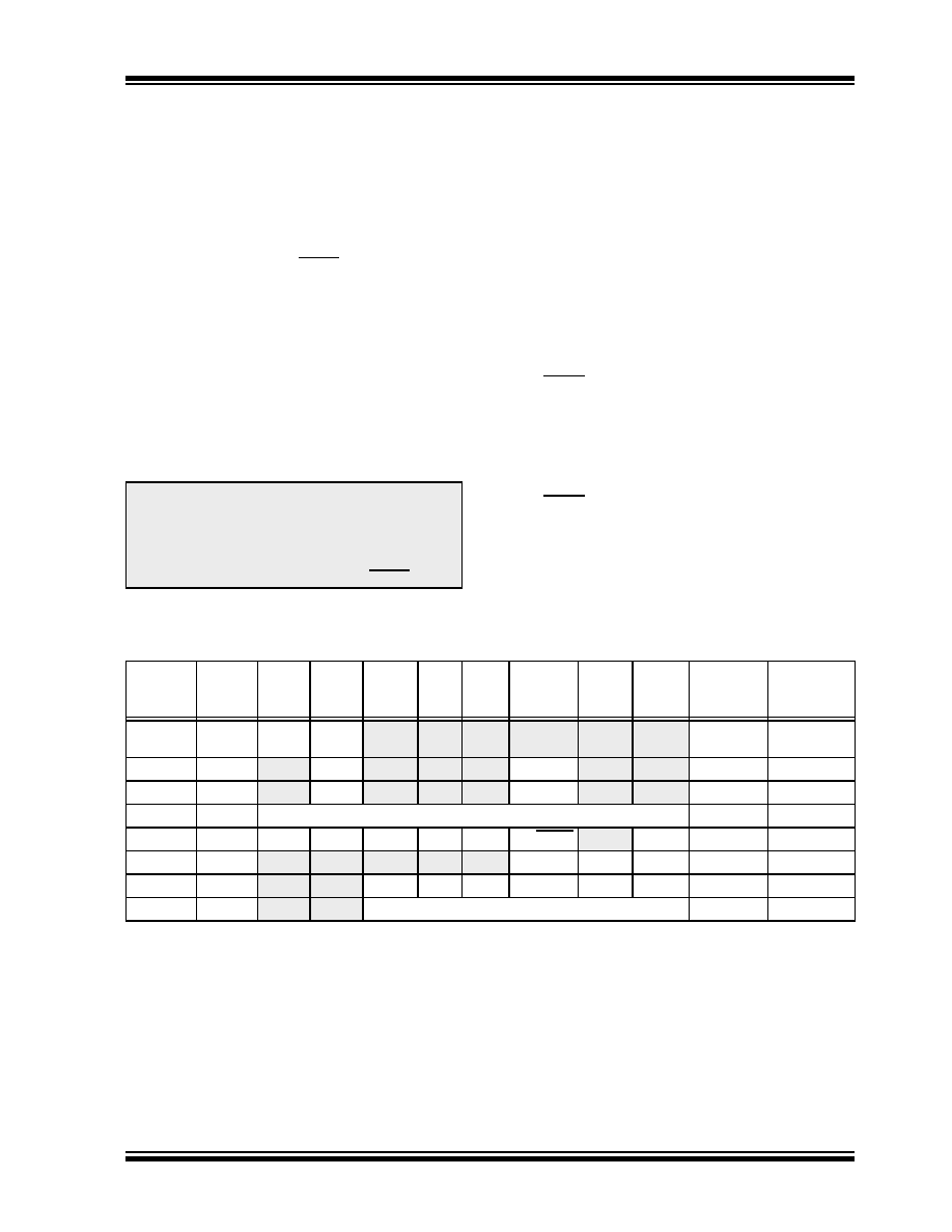
TABLE 10-2:
REGISTERS/BITS ASSOCIATED WITH A/D
Note:
For the A/D module to operate in SLEEP,
the A/D clock source must be set to RC
(ADCS1:ADCS0 = 11). To perform an A/D
conversion in SLEEP, ensure the SLEEP
instruction
immediately
follows
the
instruction that sets the GO/DONE bit.
Address
Name
Bit 7
Bit 6
Bit 5
Bit 4
Bit 3
Bit 2
Bit 1
Bit 0
Value on
POR, BOR
Value on
all other
RESETS
0Bh,8Bh
10Bh,18Bh
INTCON
GIE
PEIE
TMR0IE
INTE
RBIE
TMR0IF
INTF
RBIF
0000 000x
0000 000u
0Ch
PIR1
—ADIF
—
SSPIF
CCP1IF
TMR2IF TMR1IF
-0-- 0000
8Ch
PIE1
—ADIE
—
SSPIE
CCP1IE
TMR2IE TMR1IE -0-- 0000
-0-- 0000
1Eh
ADRES
A/D Result Register
xxxx xxxx
uuuu uuuu
1Fh
ADCON0
ADCS1 ADCS0
CHS2
CHS1
CHS0
GO/DONE
—ADON
0000 00-0
9Fh
ADCON1
—
PCFG2
PCFG1
PCFG0
---- -000
05h
PORTA
—
RA5
RA4
RA3
RA2
RA1
RA0
--0x 0000
--0u 0000
85h
TRISA
—
PORTA Data Direction Register
--11 1111
Legend: x = unknown, u = unchanged, - = unimplemented, read as ‘0’. Shaded cells are not used for A/D conversion.
相关PDF资料 |
PDF描述 |
|---|---|
| VI-JTH-IX-S | CONVERTER MOD DC/DC 52V 75W |
| VE-203-IY-B1 | CONVERTER MOD DC/DC 24V 50W |
| VI-JT3-IX-S | CONVERTER MOD DC/DC 24V 75W |
| PIC16LF72-I/SS | IC PIC MCU FLASH 2KX14 28SSOP |
| VI-J74-IX-S | CONVERTER MOD DC/DC 48V 75W |
相关代理商/技术参数 |
参数描述 |
|---|---|
| PIC16LF737-I/ML | 功能描述:8位微控制器 -MCU 7KB 368 RAM 25 I/O RoHS:否 制造商:Silicon Labs 核心:8051 处理器系列:C8051F39x 数据总线宽度:8 bit 最大时钟频率:50 MHz 程序存储器大小:16 KB 数据 RAM 大小:1 KB 片上 ADC:Yes 工作电源电压:1.8 V to 3.6 V 工作温度范围:- 40 C to + 105 C 封装 / 箱体:QFN-20 安装风格:SMD/SMT |
| PIC16LF737-I/SO | 功能描述:8位微控制器 -MCU 7KB 368 RAM 25 I/O RoHS:否 制造商:Silicon Labs 核心:8051 处理器系列:C8051F39x 数据总线宽度:8 bit 最大时钟频率:50 MHz 程序存储器大小:16 KB 数据 RAM 大小:1 KB 片上 ADC:Yes 工作电源电压:1.8 V to 3.6 V 工作温度范围:- 40 C to + 105 C 封装 / 箱体:QFN-20 安装风格:SMD/SMT |
| PIC16LF737-I/SP | 功能描述:8位微控制器 -MCU 7KB 368 RAM 25 I/O RoHS:否 制造商:Silicon Labs 核心:8051 处理器系列:C8051F39x 数据总线宽度:8 bit 最大时钟频率:50 MHz 程序存储器大小:16 KB 数据 RAM 大小:1 KB 片上 ADC:Yes 工作电源电压:1.8 V to 3.6 V 工作温度范围:- 40 C to + 105 C 封装 / 箱体:QFN-20 安装风格:SMD/SMT |
| PIC16LF737-I/SS | 功能描述:8位微控制器 -MCU 7KB 368 RAM 25 I/O RoHS:否 制造商:Silicon Labs 核心:8051 处理器系列:C8051F39x 数据总线宽度:8 bit 最大时钟频率:50 MHz 程序存储器大小:16 KB 数据 RAM 大小:1 KB 片上 ADC:Yes 工作电源电压:1.8 V to 3.6 V 工作温度范围:- 40 C to + 105 C 封装 / 箱体:QFN-20 安装风格:SMD/SMT |
| PIC16LF737T-I/ML | 功能描述:8位微控制器 -MCU 7KB 368 RAM 25 I/O RoHS:否 制造商:Silicon Labs 核心:8051 处理器系列:C8051F39x 数据总线宽度:8 bit 最大时钟频率:50 MHz 程序存储器大小:16 KB 数据 RAM 大小:1 KB 片上 ADC:Yes 工作电源电压:1.8 V to 3.6 V 工作温度范围:- 40 C to + 105 C 封装 / 箱体:QFN-20 安装风格:SMD/SMT |
发布紧急采购,3分钟左右您将得到回复。