- 您现在的位置:买卖IC网 > PDF目录11515 > PIC16LF72T-I/ML (Microchip Technology)IC MCU FLASH 2KX14 LV AD 28-QFN PDF资料下载
参数资料
| 型号: | PIC16LF72T-I/ML |
| 厂商: | Microchip Technology |
| 文件页数: | 86/136页 |
| 文件大小: | 0K |
| 描述: | IC MCU FLASH 2KX14 LV AD 28-QFN |
| 产品培训模块: | Asynchronous Stimulus |
| 标准包装: | 1,600 |
| 系列: | PIC® 16F |
| 核心处理器: | PIC |
| 芯体尺寸: | 8-位 |
| 速度: | 20MHz |
| 连通性: | I²C,SPI |
| 外围设备: | 欠压检测/复位,POR,PWM,WDT |
| 输入/输出数: | 22 |
| 程序存储器容量: | 3.5KB(2K x 14) |
| 程序存储器类型: | 闪存 |
| RAM 容量: | 128 x 8 |
| 电压 - 电源 (Vcc/Vdd): | 2 V ~ 5.5 V |
| 数据转换器: | A/D 5x8b |
| 振荡器型: | 外部 |
| 工作温度: | -40°C ~ 85°C |
| 封装/外壳: | 28-VQFN 裸露焊盘 |
| 包装: | 带卷 (TR) |
第1页第2页第3页第4页第5页第6页第7页第8页第9页第10页第11页第12页第13页第14页第15页第16页第17页第18页第19页第20页第21页第22页第23页第24页第25页第26页第27页第28页第29页第30页第31页第32页第33页第34页第35页第36页第37页第38页第39页第40页第41页第42页第43页第44页第45页第46页第47页第48页第49页第50页第51页第52页第53页第54页第55页第56页第57页第58页第59页第60页第61页第62页第63页第64页第65页第66页第67页第68页第69页第70页第71页第72页第73页第74页第75页第76页第77页第78页第79页第80页第81页第82页第83页第84页第85页当前第86页第87页第88页第89页第90页第91页第92页第93页第94页第95页第96页第97页第98页第99页第100页第101页第102页第103页第104页第105页第106页第107页第108页第109页第110页第111页第112页第113页第114页第115页第116页第117页第118页第119页第120页第121页第122页第123页第124页第125页第126页第127页第128页第129页第130页第131页第132页第133页第134页第135页第136页
2007 Microchip Technology Inc.
DS39597C-page 51
PIC16F72
9.3.2
MASTER MODE OPERATION
Master mode operation is supported in firmware using
interrupt generation on the detection of the START and
STOP conditions. The STOP (P) and START (S) bits
are cleared from a RESET or when the SSP module is
disabled. The STOP (P) and START (S) bits will toggle,
based on the START and STOP conditions. Control of
the I2C bus may be taken when the P bit is set, or the
bus is IDLE and both the S and P bits are clear.
In Master mode operation, the SCL and SDA lines are
manipulated in firmware by clearing the corresponding
TRISC<4:3> bit(s). The output level is always low, irre-
spective of the value(s) in PORTC<4:3>. So, when
transmitting data, a ‘1’ data bit must have the
TRISC<4> bit set (input) and a ‘0’ data bit must have
the TRISC<4> bit cleared (output). The same scenario
is true for the SCL line with the TRISC<3> bit.
The following events will cause the SSP Interrupt Flag
bit, SSPIF, to be set (SSP Interrupt if enabled):
START condition
STOP condition
Data transfer byte transmitted/received
Master mode operation can be done with either the
Slave mode IDLE (SSPM3:SSPM0 = 1011), or with the
Slave mode active. When both Master mode operation
and Slave modes are used, the software needs to
differentiate the source(s) of the interrupt.
For more information on Master mode operation, see
AN554 - Software Implementation of I2C Bus Master.
9.3.3
MULTI-MASTER MODE OPERATION
In Multi-Master mode operation, the interrupt genera-
tion on the detection of the START and STOP condi-
tions allows the determination of when the bus is free.
The STOP (P) and START (S) bits are cleared from a
RESET or when the SSP module is disabled. The
STOP (P) and START (S) bits will toggle, based on the
START and STOP conditions. Control of the I2C bus
may be taken when bit P (SSPSTAT<4>) is set, or the
bus is IDLE and both the S and P bits clear. When the
bus is busy, enabling the SSP interrupt will generate
the interrupt when the STOP condition occurs.
In Multi-Master mode operation, the SDA line must be
monitored to see if the signal level is the expected out-
put level. This check only needs to be done when a
high level is output. If a high level is expected and a low
level is present, the device needs to release the SDA
and SCL lines (set TRISC<4:3>). There are two stages
where this arbitration can be lost:
Address Transfer
Data Transfer
When the slave logic is enabled, the Slave device con-
tinues to receive. If arbitration was lost during the
address transfer stage, communication to the device
may be in progress. If addressed, an ACK pulse will be
generated. If arbitration was lost during the data trans-
fer stage, the device will need to retransfer the data at
a later time.
For more information on Multi-Master mode operation,
see AN578 - Use of the SSP Module in the I2C
Multi-Master Environment.
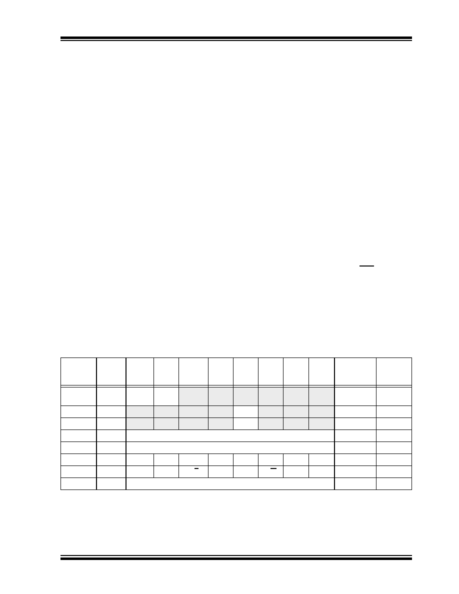
TABLE 9-3:
REGISTERS ASSOCIATED WITH I2C OPERATION
Address
Name
Bit 7
Bit 6
Bit 5
Bit 4
Bit 3
Bit 2
Bit 1
Bit 0
Value on
POR, BOR
Value on
all other
RESETS
0Bh, 8Bh,
10Bh,18Bh
INTCON
GIE
PEIE
TMR0IE
INTE
RBIE
TMR0IF
INTF
RBIF
0000 000x
0000 000u
0Ch
PIR1
—
ADIF
—
—SSPIF
CCP1IF TMR2IF TMR1IF
-0-- 0000
0000 0000
8Ch
PIE1
—
ADIE
—
—SSPIE CCP1IE TMR2IE TMR1IE
-0-- 0000
0000 0000
13h
SSPBUF
Synchronous Serial Port Receive Buffer/Transmit Register
xxxx xxxx
uuuu uuuu
93h
SSPADD Synchronous Serial Port (I2C mode) Address Register
0000 0000
14h
SSPCON
WCOL
SSPOV
SSPEN
CKP
SSPM3 SSPM2 SSPM1 SSPM0
0000 0000
94h
SSPSTAT
SMP(1)
CKE(1)
D/A
PS
R/W
UA
BF
0000 0000
87h
TRISC
PORTC Data Direction Register
1111 1111
Legend: x = unknown, u = unchanged, - = unimplemented locations read as ‘0’.
Shaded cells are not used by SSP module in SPI mode.
Note
1: Maintain these bits clear in I2C mode.
相关PDF资料 |
PDF描述 |
|---|---|
| VI-JTH-IX-S | CONVERTER MOD DC/DC 52V 75W |
| VE-203-IY-B1 | CONVERTER MOD DC/DC 24V 50W |
| VI-JT3-IX-S | CONVERTER MOD DC/DC 24V 75W |
| PIC16LF72-I/SS | IC PIC MCU FLASH 2KX14 28SSOP |
| VI-J74-IX-S | CONVERTER MOD DC/DC 48V 75W |
相关代理商/技术参数 |
参数描述 |
|---|---|
| PIC16LF737-I/ML | 功能描述:8位微控制器 -MCU 7KB 368 RAM 25 I/O RoHS:否 制造商:Silicon Labs 核心:8051 处理器系列:C8051F39x 数据总线宽度:8 bit 最大时钟频率:50 MHz 程序存储器大小:16 KB 数据 RAM 大小:1 KB 片上 ADC:Yes 工作电源电压:1.8 V to 3.6 V 工作温度范围:- 40 C to + 105 C 封装 / 箱体:QFN-20 安装风格:SMD/SMT |
| PIC16LF737-I/SO | 功能描述:8位微控制器 -MCU 7KB 368 RAM 25 I/O RoHS:否 制造商:Silicon Labs 核心:8051 处理器系列:C8051F39x 数据总线宽度:8 bit 最大时钟频率:50 MHz 程序存储器大小:16 KB 数据 RAM 大小:1 KB 片上 ADC:Yes 工作电源电压:1.8 V to 3.6 V 工作温度范围:- 40 C to + 105 C 封装 / 箱体:QFN-20 安装风格:SMD/SMT |
| PIC16LF737-I/SP | 功能描述:8位微控制器 -MCU 7KB 368 RAM 25 I/O RoHS:否 制造商:Silicon Labs 核心:8051 处理器系列:C8051F39x 数据总线宽度:8 bit 最大时钟频率:50 MHz 程序存储器大小:16 KB 数据 RAM 大小:1 KB 片上 ADC:Yes 工作电源电压:1.8 V to 3.6 V 工作温度范围:- 40 C to + 105 C 封装 / 箱体:QFN-20 安装风格:SMD/SMT |
| PIC16LF737-I/SS | 功能描述:8位微控制器 -MCU 7KB 368 RAM 25 I/O RoHS:否 制造商:Silicon Labs 核心:8051 处理器系列:C8051F39x 数据总线宽度:8 bit 最大时钟频率:50 MHz 程序存储器大小:16 KB 数据 RAM 大小:1 KB 片上 ADC:Yes 工作电源电压:1.8 V to 3.6 V 工作温度范围:- 40 C to + 105 C 封装 / 箱体:QFN-20 安装风格:SMD/SMT |
| PIC16LF737T-I/ML | 功能描述:8位微控制器 -MCU 7KB 368 RAM 25 I/O RoHS:否 制造商:Silicon Labs 核心:8051 处理器系列:C8051F39x 数据总线宽度:8 bit 最大时钟频率:50 MHz 程序存储器大小:16 KB 数据 RAM 大小:1 KB 片上 ADC:Yes 工作电源电压:1.8 V to 3.6 V 工作温度范围:- 40 C to + 105 C 封装 / 箱体:QFN-20 安装风格:SMD/SMT |
发布紧急采购,3分钟左右您将得到回复。