- 您现在的位置:买卖IC网 > PDF目录11515 > PIC16LF72T-I/ML (Microchip Technology)IC MCU FLASH 2KX14 LV AD 28-QFN PDF资料下载
参数资料
| 型号: | PIC16LF72T-I/ML |
| 厂商: | Microchip Technology |
| 文件页数: | 91/136页 |
| 文件大小: | 0K |
| 描述: | IC MCU FLASH 2KX14 LV AD 28-QFN |
| 产品培训模块: | Asynchronous Stimulus |
| 标准包装: | 1,600 |
| 系列: | PIC® 16F |
| 核心处理器: | PIC |
| 芯体尺寸: | 8-位 |
| 速度: | 20MHz |
| 连通性: | I²C,SPI |
| 外围设备: | 欠压检测/复位,POR,PWM,WDT |
| 输入/输出数: | 22 |
| 程序存储器容量: | 3.5KB(2K x 14) |
| 程序存储器类型: | 闪存 |
| RAM 容量: | 128 x 8 |
| 电压 - 电源 (Vcc/Vdd): | 2 V ~ 5.5 V |
| 数据转换器: | A/D 5x8b |
| 振荡器型: | 外部 |
| 工作温度: | -40°C ~ 85°C |
| 封装/外壳: | 28-VQFN 裸露焊盘 |
| 包装: | 带卷 (TR) |
第1页第2页第3页第4页第5页第6页第7页第8页第9页第10页第11页第12页第13页第14页第15页第16页第17页第18页第19页第20页第21页第22页第23页第24页第25页第26页第27页第28页第29页第30页第31页第32页第33页第34页第35页第36页第37页第38页第39页第40页第41页第42页第43页第44页第45页第46页第47页第48页第49页第50页第51页第52页第53页第54页第55页第56页第57页第58页第59页第60页第61页第62页第63页第64页第65页第66页第67页第68页第69页第70页第71页第72页第73页第74页第75页第76页第77页第78页第79页第80页第81页第82页第83页第84页第85页第86页第87页第88页第89页第90页当前第91页第92页第93页第94页第95页第96页第97页第98页第99页第100页第101页第102页第103页第104页第105页第106页第107页第108页第109页第110页第111页第112页第113页第114页第115页第116页第117页第118页第119页第120页第121页第122页第123页第124页第125页第126页第127页第128页第129页第130页第131页第132页第133页第134页第135页第136页
PIC16F72
DS39597C-page 56
2007 Microchip Technology Inc.
10.1
A/D Acquisition Requirements
For the A/D converter to meet its specified accuracy,
the charge holding capacitor (CHOLD) must be allowed
to fully charge to the input channel voltage level. The
analog input model is shown in Figure 10-2. The
source impedance (RS) and the internal sampling
switch (RSS) impedance directly affect the time
required to charge the capacitor CHOLD. The sampling
switch (RSS) impedance varies over the device voltage
(VDD). The source impedance affects the offset voltage
at the analog input (due to pin leakage current).
The maximum recommended impedance for ana-
log sources is 10 k
Ω. After the analog input channel is
selected (changed), this acquisition must be done
before the conversion can be started.
To calculate the minimum acquisition time, TACQ, see
the PIC
Mid-Range MCU Reference Manual,
(DS33023). In general, however, given a max of 10 k
Ω
and at a temperature of 100°C, TACQ will be no more
than 16
μs.
10.2
Selecting the A/D Conversion
Clock
The A/D conversion time per bit is defined as TAD. The
A/D conversion requires 9.0 TAD per 8-bit conversion.
The source of the A/D conversion clock is software
selectable. The four possible options for TAD are:
2 TOSC
8 TOSC
32 TOSC
Internal RC oscillator (2 - 6
μs)
For correct A/D conversions, the A/D conversion clock
(TAD) must be selected to ensure a minimum TAD time
as small as possible, but no less than 1.6
μs and not
greater than 6.4
μs.
the device operating frequencies and the A/D clock
source selected.
10.3
Configuring Analog Port Pins
The ADCON1, and TRISA registers control the opera-
tion of the A/D port pins. The port pins that are desired
as analog inputs must have their corresponding TRIS
bits set (input). If the TRIS bit is cleared (output), the
digital output level (VOH or VOL) will be converted.
The A/D operation is independent of the state of the
CHS<2:0> bits and the TRIS bits.
10.4
A/D Conversions
Clearing the GO/DONE bit during a conversion will
abort the current conversion. The ADRES register will
NOT be updated with the partially completed A/D con-
version sample. That is, the ADRES register will con-
tinue to contain the value of the last completed
conversion (or the last value written to the ADRES reg-
ister). After the A/D conversion is aborted, a 2 TAD wait
is required before the next acquisition is started. After
this 2 TAD wait, an acquisition is automatically started
on the selected channel. The GO/DONE bit can then
be set to start the conversion.
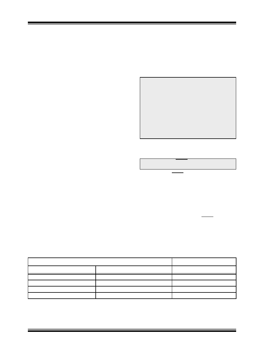
TABLE 10-1:
TAD vs. MAXIMUM DEVICE OPERATING FREQUENCIES (STANDARD DEVICES (C))
Note 1: When reading the port register, all pins
configured as analog input channels will
read as cleared (a low level). Pins config-
ured as digital inputs, will convert an
analog input. Analog levels on a digitally
configured
input
will
not
affect
the
conversion accuracy.
2: Analog levels on any pin that is defined as
a digital input (including the AN4:AN0
pins), may cause the input buffer to
consume current out of the device
specification.
Note:
The GO/DONE bit should NOT be set in
the same instruction that turns on the A/D.
AD Clock Source (TAD)
Maximum Device Frequency
Operation
ADCS<1:0>
Max.
2 TOSC
00
1.25 MHz
8 TOSC
01
5 MHz
32 TOSC
10
20 MHz
RC(1, 2)
11
(Note 1)
Note 1: The RC source has a typical TAD time of 4
μs, but can vary between 2-6 μs.
2: When the device frequencies are greater than 1 MHz, the RC A/D conversion clock source is only
recommended for SLEEP operation.
相关PDF资料 |
PDF描述 |
|---|---|
| VI-JTH-IX-S | CONVERTER MOD DC/DC 52V 75W |
| VE-203-IY-B1 | CONVERTER MOD DC/DC 24V 50W |
| VI-JT3-IX-S | CONVERTER MOD DC/DC 24V 75W |
| PIC16LF72-I/SS | IC PIC MCU FLASH 2KX14 28SSOP |
| VI-J74-IX-S | CONVERTER MOD DC/DC 48V 75W |
相关代理商/技术参数 |
参数描述 |
|---|---|
| PIC16LF737-I/ML | 功能描述:8位微控制器 -MCU 7KB 368 RAM 25 I/O RoHS:否 制造商:Silicon Labs 核心:8051 处理器系列:C8051F39x 数据总线宽度:8 bit 最大时钟频率:50 MHz 程序存储器大小:16 KB 数据 RAM 大小:1 KB 片上 ADC:Yes 工作电源电压:1.8 V to 3.6 V 工作温度范围:- 40 C to + 105 C 封装 / 箱体:QFN-20 安装风格:SMD/SMT |
| PIC16LF737-I/SO | 功能描述:8位微控制器 -MCU 7KB 368 RAM 25 I/O RoHS:否 制造商:Silicon Labs 核心:8051 处理器系列:C8051F39x 数据总线宽度:8 bit 最大时钟频率:50 MHz 程序存储器大小:16 KB 数据 RAM 大小:1 KB 片上 ADC:Yes 工作电源电压:1.8 V to 3.6 V 工作温度范围:- 40 C to + 105 C 封装 / 箱体:QFN-20 安装风格:SMD/SMT |
| PIC16LF737-I/SP | 功能描述:8位微控制器 -MCU 7KB 368 RAM 25 I/O RoHS:否 制造商:Silicon Labs 核心:8051 处理器系列:C8051F39x 数据总线宽度:8 bit 最大时钟频率:50 MHz 程序存储器大小:16 KB 数据 RAM 大小:1 KB 片上 ADC:Yes 工作电源电压:1.8 V to 3.6 V 工作温度范围:- 40 C to + 105 C 封装 / 箱体:QFN-20 安装风格:SMD/SMT |
| PIC16LF737-I/SS | 功能描述:8位微控制器 -MCU 7KB 368 RAM 25 I/O RoHS:否 制造商:Silicon Labs 核心:8051 处理器系列:C8051F39x 数据总线宽度:8 bit 最大时钟频率:50 MHz 程序存储器大小:16 KB 数据 RAM 大小:1 KB 片上 ADC:Yes 工作电源电压:1.8 V to 3.6 V 工作温度范围:- 40 C to + 105 C 封装 / 箱体:QFN-20 安装风格:SMD/SMT |
| PIC16LF737T-I/ML | 功能描述:8位微控制器 -MCU 7KB 368 RAM 25 I/O RoHS:否 制造商:Silicon Labs 核心:8051 处理器系列:C8051F39x 数据总线宽度:8 bit 最大时钟频率:50 MHz 程序存储器大小:16 KB 数据 RAM 大小:1 KB 片上 ADC:Yes 工作电源电压:1.8 V to 3.6 V 工作温度范围:- 40 C to + 105 C 封装 / 箱体:QFN-20 安装风格:SMD/SMT |
发布紧急采购,3分钟左右您将得到回复。