- 您现在的位置:买卖IC网 > PDF目录1965 > PIC18LF2450T-I/SO (Microchip Technology)IC PIC MCU FLASH 8KX16 28SOIC PDF资料下载
参数资料
| 型号: | PIC18LF2450T-I/SO |
| 厂商: | Microchip Technology |
| 文件页数: | 116/143页 |
| 文件大小: | 0K |
| 描述: | IC PIC MCU FLASH 8KX16 28SOIC |
| 标准包装: | 1,600 |
| 系列: | PIC® 18F |
| 核心处理器: | PIC |
| 芯体尺寸: | 8-位 |
| 速度: | 48MHz |
| 连通性: | UART/USART,USB |
| 外围设备: | 欠压检测/复位,HLVD,POR,PWM,WDT |
| 输入/输出数: | 23 |
| 程序存储器容量: | 16KB(8K x 16) |
| 程序存储器类型: | 闪存 |
| RAM 容量: | 768 x 8 |
| 电压 - 电源 (Vcc/Vdd): | 2 V ~ 5.5 V |
| 数据转换器: | A/D 10x10b |
| 振荡器型: | 内部 |
| 工作温度: | -40°C ~ 85°C |
| 封装/外壳: | 28-SOIC(0.295",7.50mm 宽) |
| 包装: | 带卷 (TR) |
第1页第2页第3页第4页第5页第6页第7页第8页第9页第10页第11页第12页第13页第14页第15页第16页第17页第18页第19页第20页第21页第22页第23页第24页第25页第26页第27页第28页第29页第30页第31页第32页第33页第34页第35页第36页第37页第38页第39页第40页第41页第42页第43页第44页第45页第46页第47页第48页第49页第50页第51页第52页第53页第54页第55页第56页第57页第58页第59页第60页第61页第62页第63页第64页第65页第66页第67页第68页第69页第70页第71页第72页第73页第74页第75页第76页第77页第78页第79页第80页第81页第82页第83页第84页第85页第86页第87页第88页第89页第90页第91页第92页第93页第94页第95页第96页第97页第98页第99页第100页第101页第102页第103页第104页第105页第106页第107页第108页第109页第110页第111页第112页第113页第114页第115页当前第116页第117页第118页第119页第120页第121页第122页第123页第124页第125页第126页第127页第128页第129页第130页第131页第132页第133页第134页第135页第136页第137页第138页第139页第140页第141页第142页第143页
PIC18F2450/4450
DS39760A-page 72
Advance Information
2006 Microchip Technology Inc.
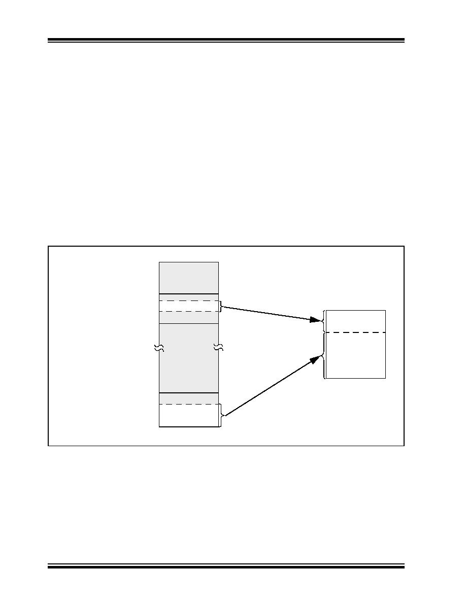
5.6.3
MAPPING THE ACCESS BANK IN
INDEXED LITERAL OFFSET MODE
The use of Indexed Literal Offset Addressing mode
effectively changes how the lower portion of Access
RAM (00h to 5Fh) is mapped. Rather than containing
just the contents of the bottom half of Bank 0, this mode
maps the contents from Bank 0 and a user-defined
“window” that can be located anywhere in the data
memory space. The value of FSR2 establishes the
lower boundary of the addresses mapped into the
window, while the upper boundary is defined by FSR2
plus 95 (5Fh). Addresses in the Access RAM above
5Fh are mapped as previously described (see
Section 5.3.3 “Access Bank”). An example of Access
Bank remapping in this addressing mode is shown in
Remapping of the Access Bank applies
only to
operations using the Indexed Literal Offset mode.
Operations that use the BSR (Access RAM bit is ‘1’) will
continue to use Direct Addressing as before. Any
indirect or indexed operation that explicitly uses any of
the indirect file operands (including FSR2) will continue
to operate as standard Indirect Addressing. Any
instruction that uses the Access Bank, but includes a
register address of greater than 05Fh, will use Direct
Addressing and the normal Access Bank map.
5.6.4
BSR IN INDEXED LITERAL
OFFSET MODE
Although the Access Bank is remapped when the
extended instruction set is enabled, the operation of the
BSR remains unchanged. Direct Addressing, using the
BSR to select the data memory bank, operates in the
same manner as previously described.
FIGURE 5-9:
REMAPPING THE ACCESS BANK WITH INDEXED LITERAL
OFFSET ADDRESSING
Data Memory
000h
100h
200h
F60h
F00h
FFFh
Bank 1
Bank 15
Bank 2
through
Bank 14
SFRs
ADDWF f, d, a
FSR2H:FSR2L = 120h
Locations in the region
from the FSR2 Pointer
(120h) to the pointer plus
05Fh (17Fh) are mapped
to
the
bottom
of
the
Access RAM (000h-05Fh).
Special Function Regis-
ters at F60h through FFFh
are
mapped
to
60h
through FFh as usual.
Bank 0 addresses below
5Fh are not available in
this mode. They can still
be addressed by using the
BSR.
Access Bank
00h
60h
FFh
Bank 0
SFRs
Bank 1 “Window”
Window
Example Situation:
120h
17Fh
5Fh
相关PDF资料 |
PDF描述 |
|---|---|
| PIC18LF4320-I/PT | IC MCU FLASH 4KX16 EEPROM 44TQFP |
| PIC18LF4321-I/ML | IC PIC MCU FLASH 4KX16 44QFN |
| PIC18LF4431-I/ML | IC PIC MCU FLASH 8KX16 44QFN |
| PIC18LF44J10-I/P | IC PIC MCU FLASH 8KX16 40DIP |
| PIC18LF452-I/ML | IC MCU FLASH 16KX16 A/D 44QFN |
相关代理商/技术参数 |
参数描述 |
|---|---|
| PIC18LF2455-I/SO | 功能描述:8位微控制器 -MCU 24kBF 2048RM FSUSB2 RoHS:否 制造商:Silicon Labs 核心:8051 处理器系列:C8051F39x 数据总线宽度:8 bit 最大时钟频率:50 MHz 程序存储器大小:16 KB 数据 RAM 大小:1 KB 片上 ADC:Yes 工作电源电压:1.8 V to 3.6 V 工作温度范围:- 40 C to + 105 C 封装 / 箱体:QFN-20 安装风格:SMD/SMT |
| PIC18LF2455-I/SP | 功能描述:8位微控制器 -MCU 24kBF 2048RM FSUSB2 RoHS:否 制造商:Silicon Labs 核心:8051 处理器系列:C8051F39x 数据总线宽度:8 bit 最大时钟频率:50 MHz 程序存储器大小:16 KB 数据 RAM 大小:1 KB 片上 ADC:Yes 工作电源电压:1.8 V to 3.6 V 工作温度范围:- 40 C to + 105 C 封装 / 箱体:QFN-20 安装风格:SMD/SMT |
| PIC18LF2455-I/SP | 制造商:Microchip Technology Inc 功能描述:8 Bit Microcontroller Clock Speed:48MHz |
| PIC18LF2455T-I/SO | 功能描述:8位微控制器 -MCU 24kBF 2048RM FSUSB2 RoHS:否 制造商:Silicon Labs 核心:8051 处理器系列:C8051F39x 数据总线宽度:8 bit 最大时钟频率:50 MHz 程序存储器大小:16 KB 数据 RAM 大小:1 KB 片上 ADC:Yes 工作电源电压:1.8 V to 3.6 V 工作温度范围:- 40 C to + 105 C 封装 / 箱体:QFN-20 安装风格:SMD/SMT |
| PIC18LF2458-I/SO | 功能描述:8位微控制器 -MCU 24KB Flash 2KB RAM RoHS:否 制造商:Silicon Labs 核心:8051 处理器系列:C8051F39x 数据总线宽度:8 bit 最大时钟频率:50 MHz 程序存储器大小:16 KB 数据 RAM 大小:1 KB 片上 ADC:Yes 工作电源电压:1.8 V to 3.6 V 工作温度范围:- 40 C to + 105 C 封装 / 箱体:QFN-20 安装风格:SMD/SMT |
发布紧急采购,3分钟左右您将得到回复。